


Professional custom electronics pcb board designer pcb design circuit boards one stop service electronic Assembly Manufacturer
Product Details:
- Silkscreen White, Black, Yellow options
- Board Type Rigid, Flexible, Rigid-Flex
- Min. Line Width 0.075 mm
- Soldermask Green, Blue, Red, Black, White, Yellow
- Min. Line Spacing 0.075 mm
- Test 100% E-test & AOI supported
- Impedance Controlled impedance available
- Click to view more
X
Professional custom electronics pcb board designer pcb design circuit boards one stop service electronic Assembly Manufacturer Price And Quantity
- 1
- INR
- Turnkey or consigned
- Sample 3-5 days, Mass production 5-8 days
- ISO9001, UL, RoHS, IPC
- Vacuum and ESD packaging
- Up to 01005 chip size, BGA, QFN, etc.
- Gerber, BOM, Centroid, ODB++
- One-stop service including PCB, components sourcing, and assembly
- Laser-cut stencil available
Professional custom electronics pcb board designer pcb design circuit boards one stop service electronic Assembly Manufacturer Product Specifications
- 1-20 Layers
- Rigid, Flexible, Rigid-Flex
- 1-3 oz
- Min 0.2 mm
- 0.2 mm-3.2 mm
- Green, Blue, Red, Black, White, Yellow
- 0.075 mm
- Controlled impedance available
- UL94-V0
- Customizable as per requirement
- White, Black, Yellow options
- >10^12
- Up to 3000V AC
- 0.075 mm
- FR-4, CEM-1, High TG, Aluminum, Rogers, Polyimide
- 100% E-test & AOI supported
- SMT & THT components supported
- Available per application requirements
- Professional custom electronics PCB board designer
- HASL, ENIG, OSP, Immersion Silver, Tin
- Green, Blue, Black, Red, Yellow, White options
- Turnkey or consigned
- Sample 3-5 days, Mass production 5-8 days
- ISO9001, UL, RoHS, IPC
- Vacuum and ESD packaging
- Up to 01005 chip size, BGA, QFN, etc.
- Gerber, BOM, Centroid, ODB++
- One-stop service including PCB, components sourcing, and assembly
- Laser-cut stencil available
Product Description
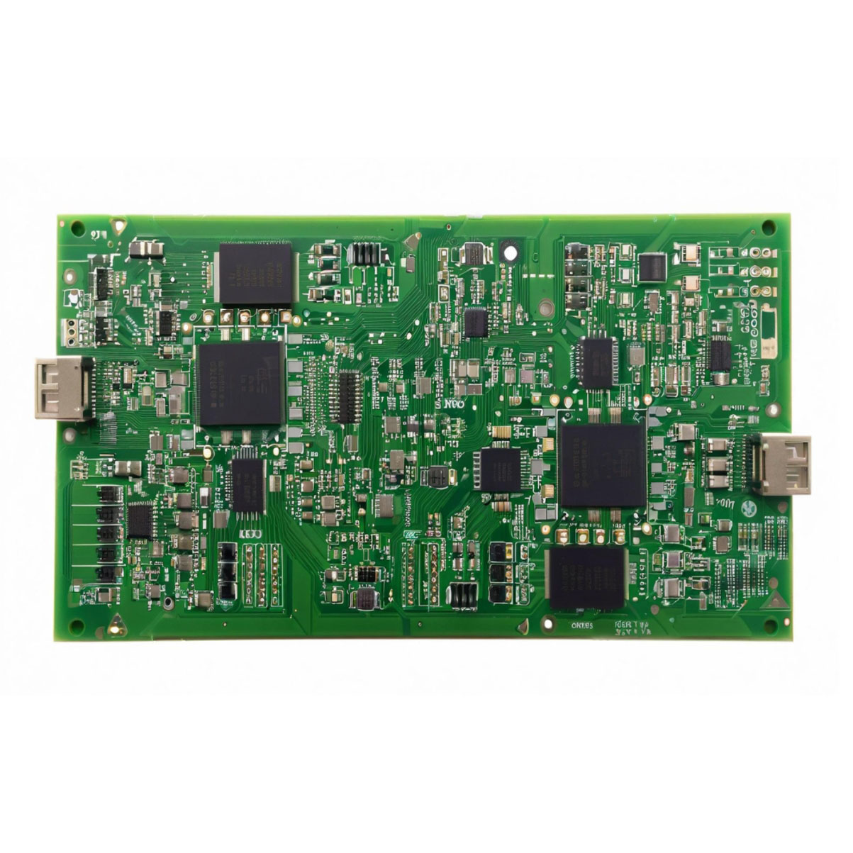
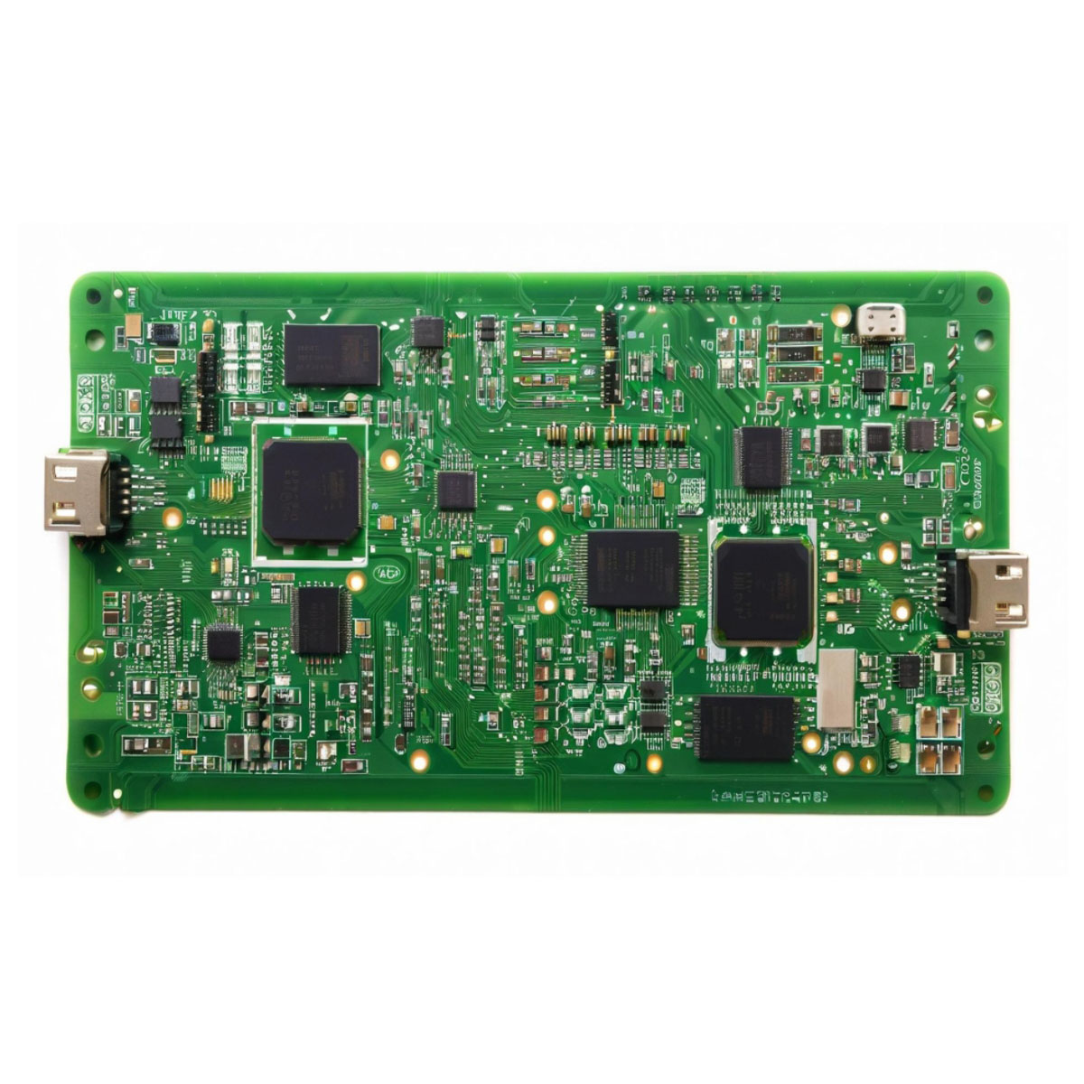
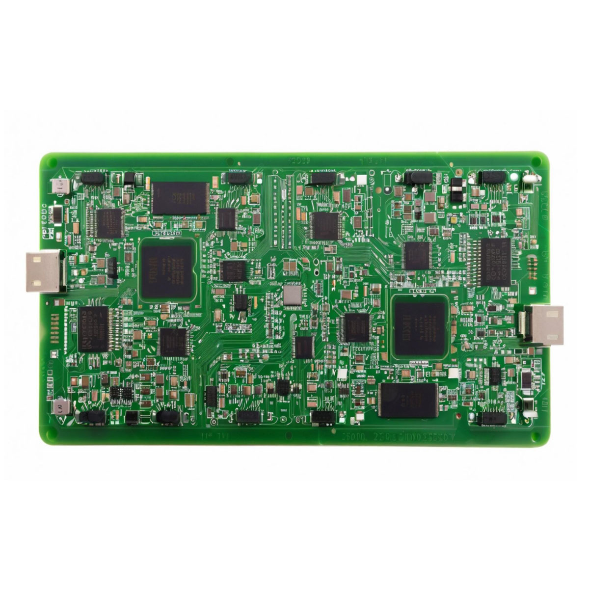
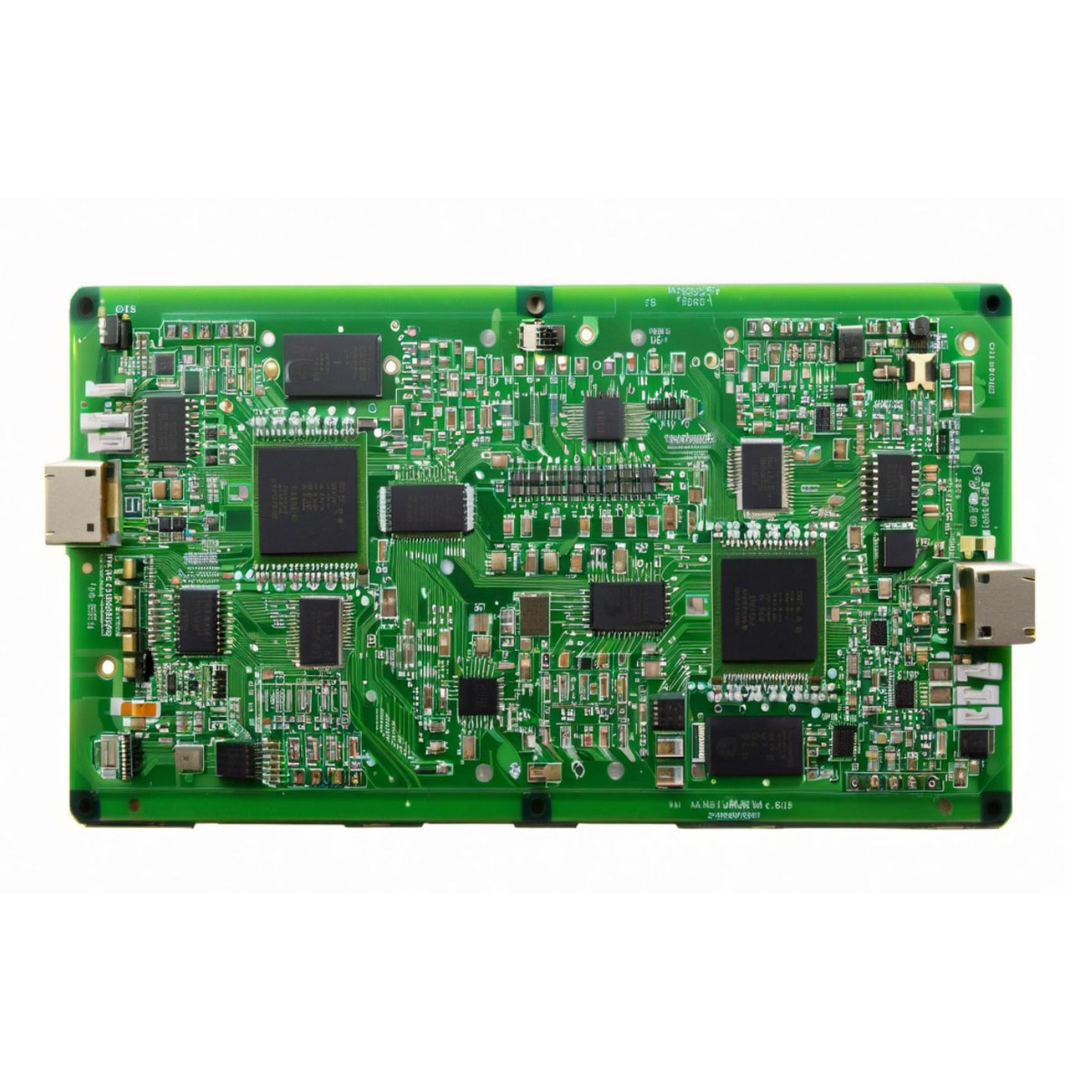
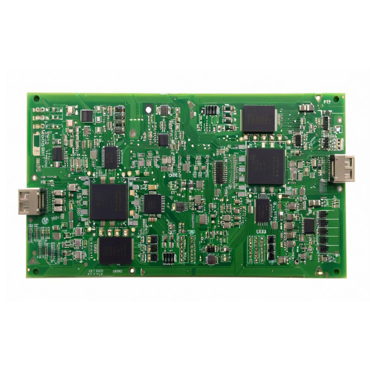
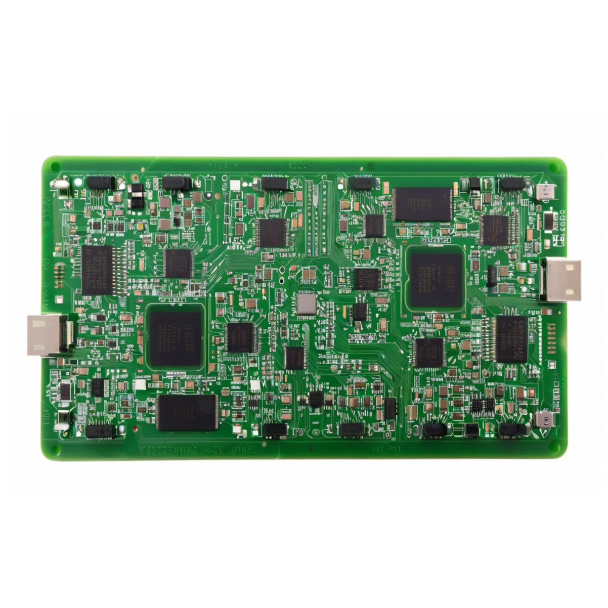
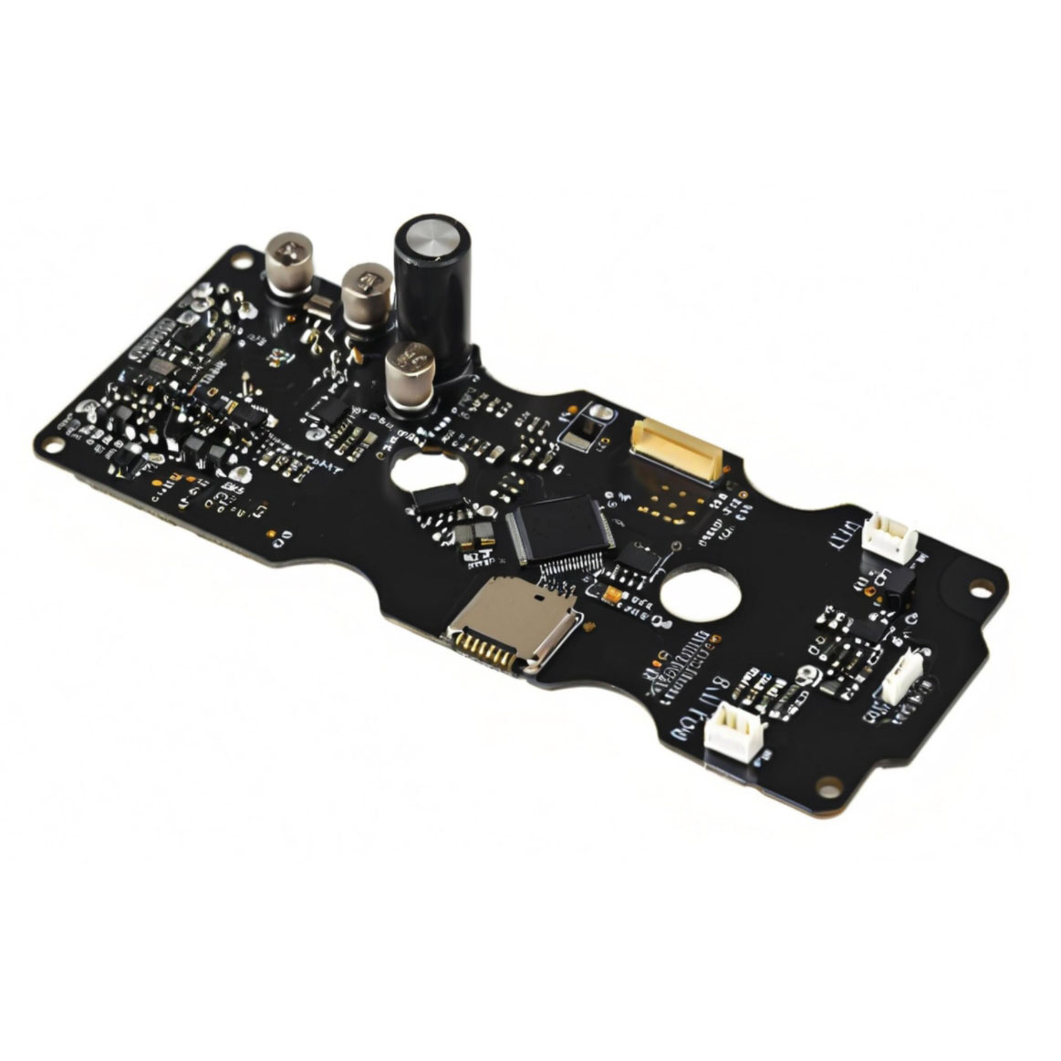
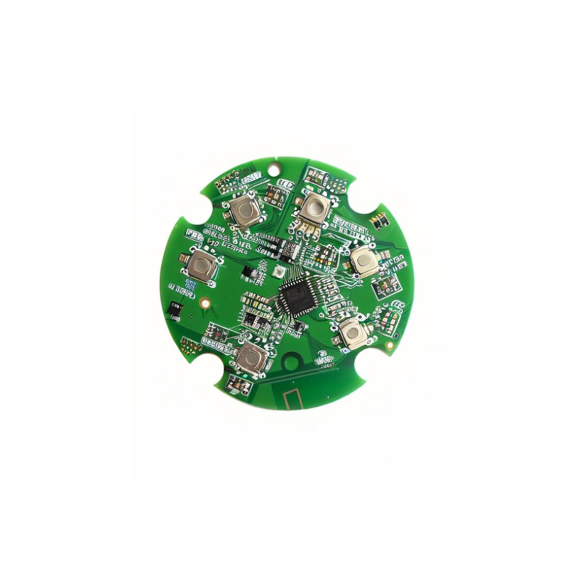
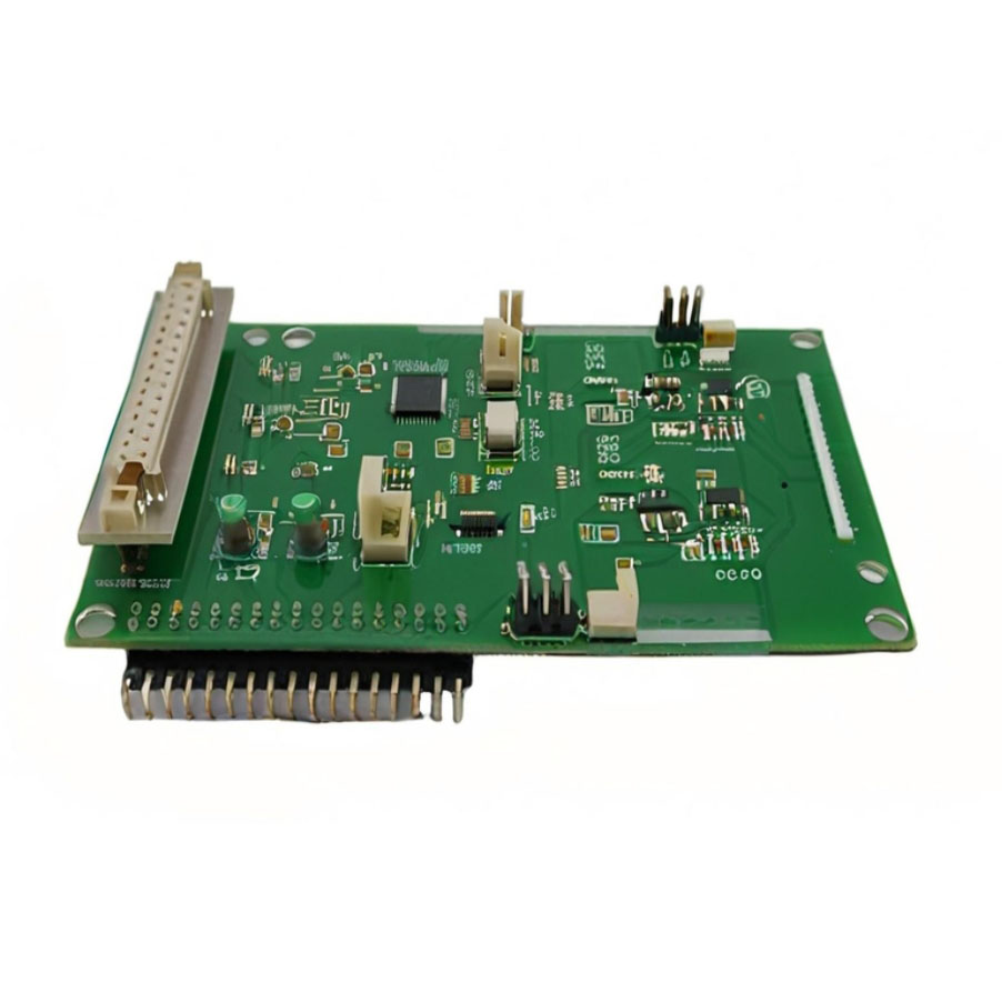
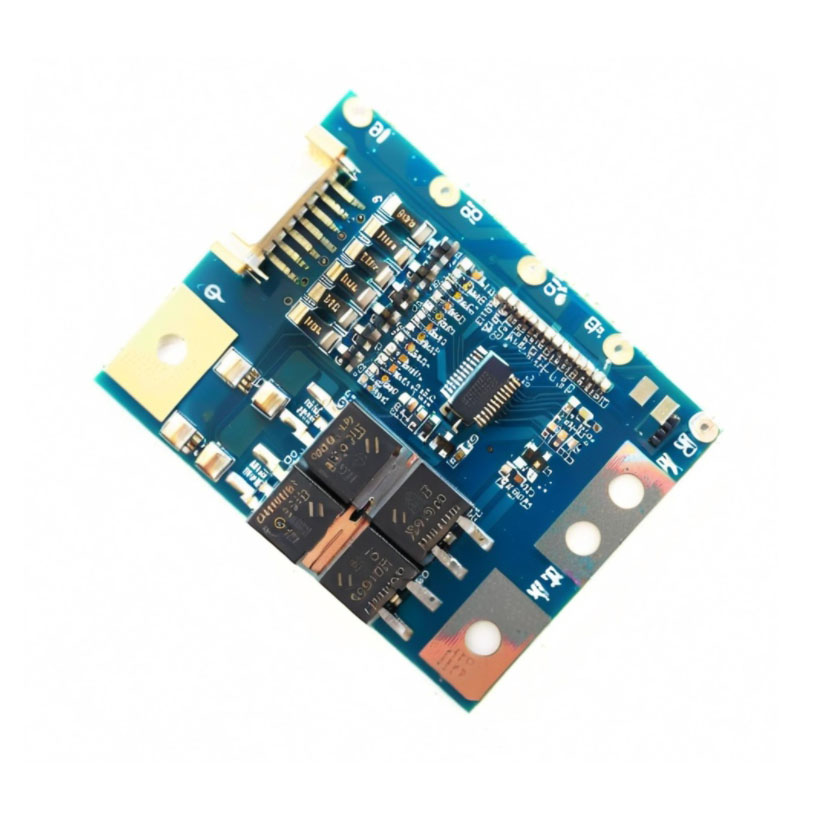
Ending Soon: Redeem the prodigious opportunity to collaborate with a heroic, featured PCB design and assembly manufacturer in India. Our one-stop service covers everything from professional custom circuit board design to world-class electronic assembly. With a best-in-class lead time-samples ready in just 3-5 days and mass production in 5-8 days-ensure speed without compromising precision. We support SMT & THT, a spectrum of materials, controlled impedance, and up to 20 layers. Experience superior workmanship, robust certifications, and versatile customization. Secure your project with our premier all-in-one solution before time runs out!
Striking Extra Features & Adaptable Applications
Our professional PCB design and assembly services include advanced options like custom panel sizes, laser-cut stencils, and controlled impedance. Whether for industrial controls, medical devices, telecom equipment, or consumer electronics, our solutions are tailored for wide-ranging applications. Benefit from select electrical components, multiple solder mask and silkscreen color choices, and versatile board types-rigid, flexible, or rigid-flex. Additional offerings include sensor switches and precise, high-reliability test methods to ensure even your most demanding projects are met with excellence.
Seamless Order Processing, Payment, and Delivery
Our streamlined order processing ensures your circuit boards are quickly shipped following a transparent list price quotation. Payment terms are flexible, catering to clients both locally and internationally. Samples are available, enabling evaluation prior to mass orders. With substantial supply ability, we can handle both small and large-scale projects efficiently. Each shipment is carefully vacuum-sealed and ESD-packed to guarantee product safety and reliability from our facility in India to your door.
FAQ's of Professional custom electronics pcb board designer pcb design circuit boards one stop service electronic Assembly Manufacturer:
Q: How does your one-stop PCB assembly service benefit my project?
A: Our one-stop solution covers everything from PCB design and component sourcing to assembly and testing-saving you time, reducing overhead, and ensuring seamless quality control for every stage of your project.Q: What file formats are supported for submitting my PCB design?
A: We accept Gerber, BOM, Centroid, ODB++, and other standard formats to streamline the transition from design to manufacturing.Q: When will my sample and mass production orders be shipped?
A: Samples are typically completed within 3-5 days, while mass production orders take about 5-8 days before shipping.Q: Where is your PCB manufacturing and assembly facility located?
A: Our advanced manufacturing and assembly facility is based in India, enabling both domestic and international shipments.Q: What are the typical payment terms and is a sample option available?
A: We offer flexible payment options and provide a sample service, so you can evaluate product quality before proceeding with full-scale orders.Q: How do you ensure product quality and safety during delivery?
A: Each board undergoes 100% E-test & AOI, is certified (ISO9001, UL, RoHS, IPC), and is vacuum and ESD-packed to ensure optimal condition upon arrival.Tell us about your requirement

Price:
Quantity
Select Unit
- 50
- 100
- 200
- 250
- 500
- 1000+
Additional detail
Mobile number
Email

Other Products in 'PCBA Customized' category
Contact Details
- No. 1506,15 Floor, SSG Tower, 561 ADien Bien Phu Str, Ward 25, Binh Thanh Dist, HCMC, Ho Chi Minh City - 717000, Thanh Pho Ho Chi Minh, Vietnam
- Ms. Yolanda Ke (Sales Account Manager)
- Mobile : +8613751081371
- Send Inquiry
NOVA TECHNOLOGY VIETNAMESE COMPANY LIMITED
|
 Call Me Free

NOVA TECHNOLOGY VIETNAMESE COMPANY LIMITED
All Rights Reserved.(Terms of Use)
Developed and Managed by Infocom Network Private Limited.
Developed and Managed by Infocom Network Private Limited.
