


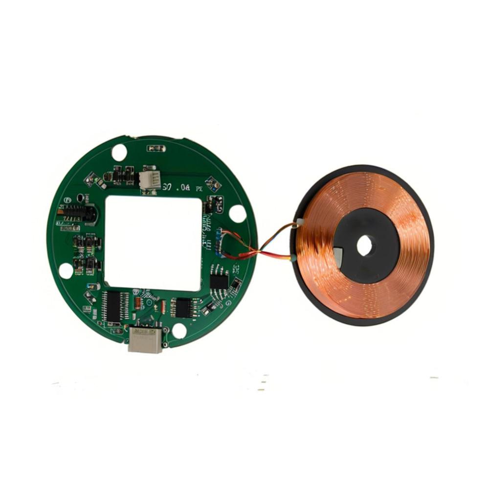
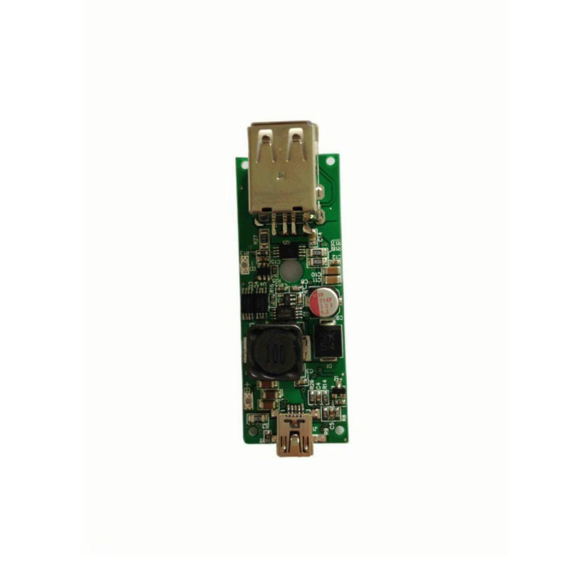
One Stop Electronic OEM PCB Circuit Board Soldering Service Smart Devices Firmware Development and PCB Design
Product Details:
- Soldermask Green, Blue, Black, Red (UV Curable)
- Impedance Controlled Impedance Available
- Min. Line Width 0.1mm
- Board Type Single Sided, Double Sided, Multilayer
- Insulation Resistance >10^12
- Min. Line Spacing 0.1mm
- Silkscreen White, Yellow (custom options)
- Click to view more
X
One Stop Electronic OEM PCB Circuit Board Soldering Service Smart Devices Firmware Development and PCB Design Price And Quantity
- 1
- INR
- Altium, Eagle, OrCAD, KiCAD, Protel
- Full BOM procurement
- Gerber, BOM, Centroid, Pick & Place Files
- Yes
- Up to 100,000 pcs/month
- 5-15 Days (Depending on quantity and design)
- USB, Wi-Fi, Bluetooth (customizable for smart devices)
- Available
- Humidity, Thermal, Vibration, Salt Spray
- Turnkey, Partial Turnkey, Consignment
- Supported (Custom Embedded Firmware)
One Stop Electronic OEM PCB Circuit Board Soldering Service Smart Devices Firmware Development and PCB Design Product Specifications
- White, Yellow (custom options)
- Min. 0.2mm
- 0.1mm
- One Stop Electronic OEM PCB Circuit Board Soldering Service
- >10^12
- 1 - 12 Layers
- 0.8mm - 2.0mm
- Available (custom integration)
- Single Sided, Double Sided, Multilayer
- HASL, ENIG, OSP, Immersion Silver
- Green, Blue, Black, Red (customizable)
- 1500V AC/min
- Green, Blue, Black, Red (UV Curable)
- SMT, Through Hole, Mixed Technology
- 1oz - 3oz
- Controlled Impedance Available
- AOI, Flying Probe, Functional Test
- 0.1mm
- UL 94V-0
- FR-4, Aluminum, CEM-1, CEM-3
- Customizable as per requirement
- Altium, Eagle, OrCAD, KiCAD, Protel
- Full BOM procurement
- Gerber, BOM, Centroid, Pick & Place Files
- Yes
- Up to 100,000 pcs/month
- 5-15 Days (Depending on quantity and design)
- USB, Wi-Fi, Bluetooth (customizable for smart devices)
- Available
- Humidity, Thermal, Vibration, Salt Spray
- Turnkey, Partial Turnkey, Consignment
- Supported (Custom Embedded Firmware)
Product Description
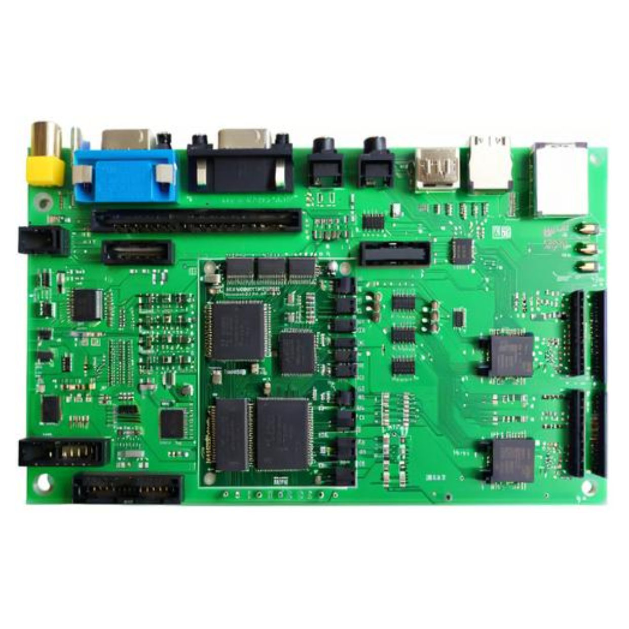
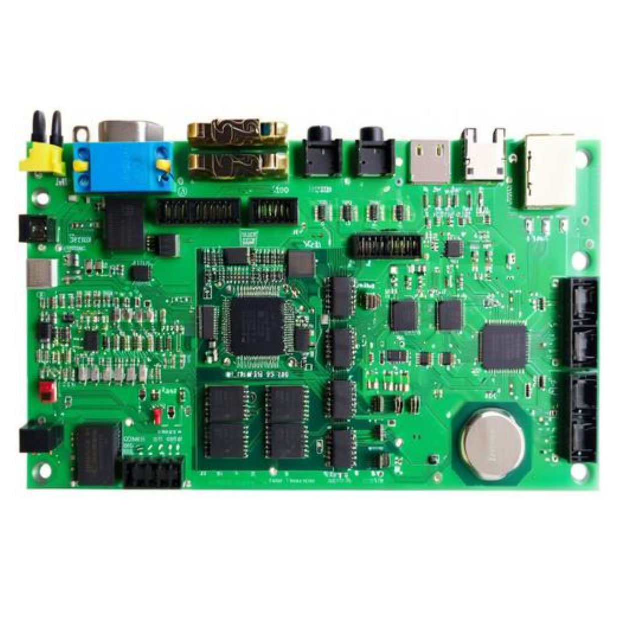
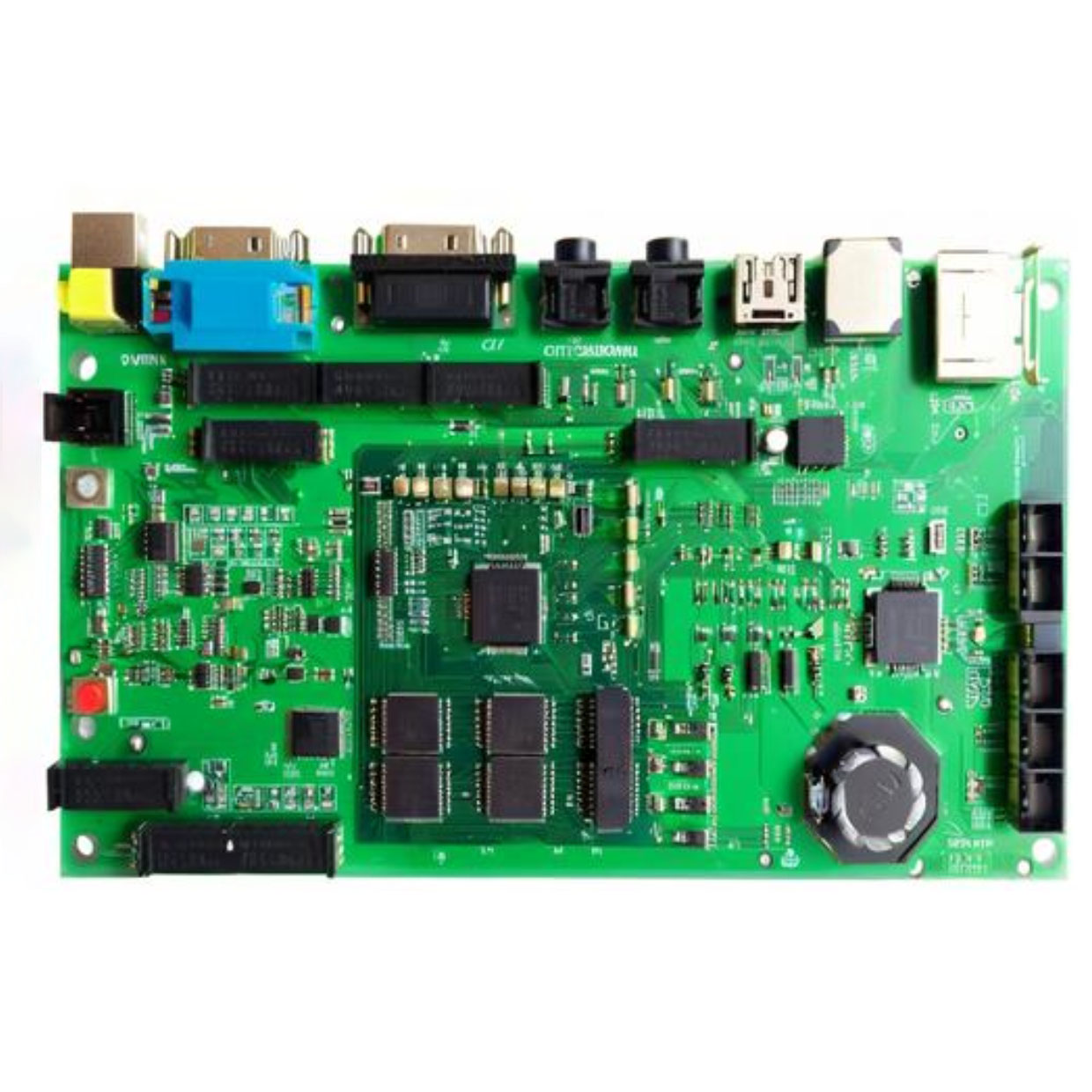
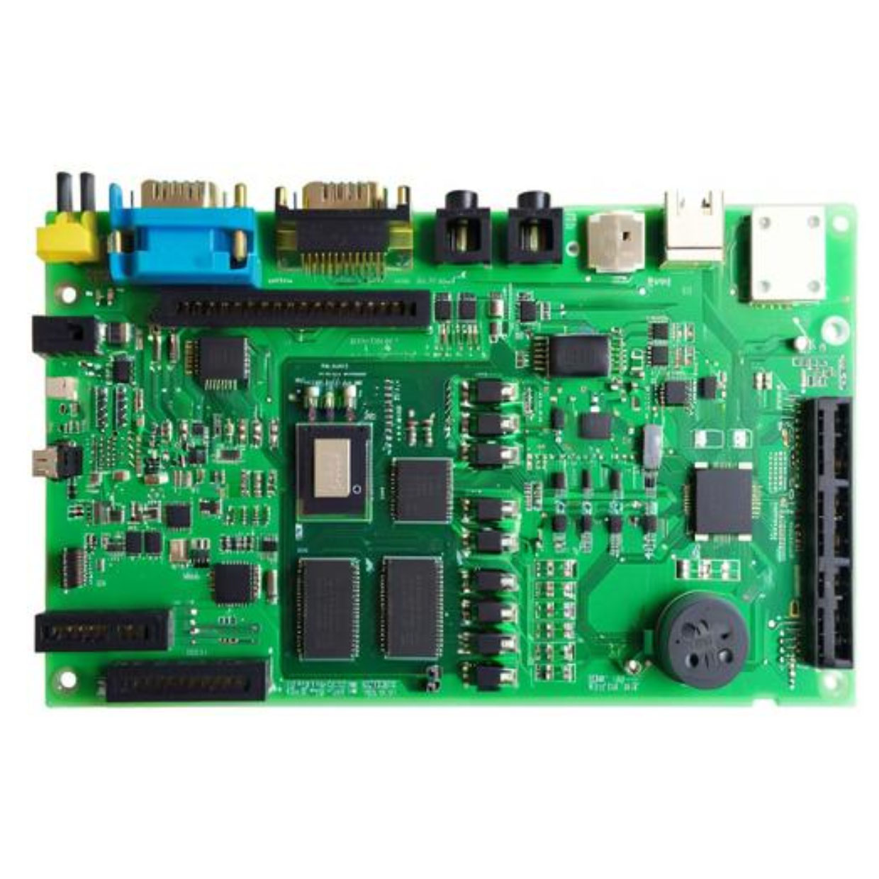
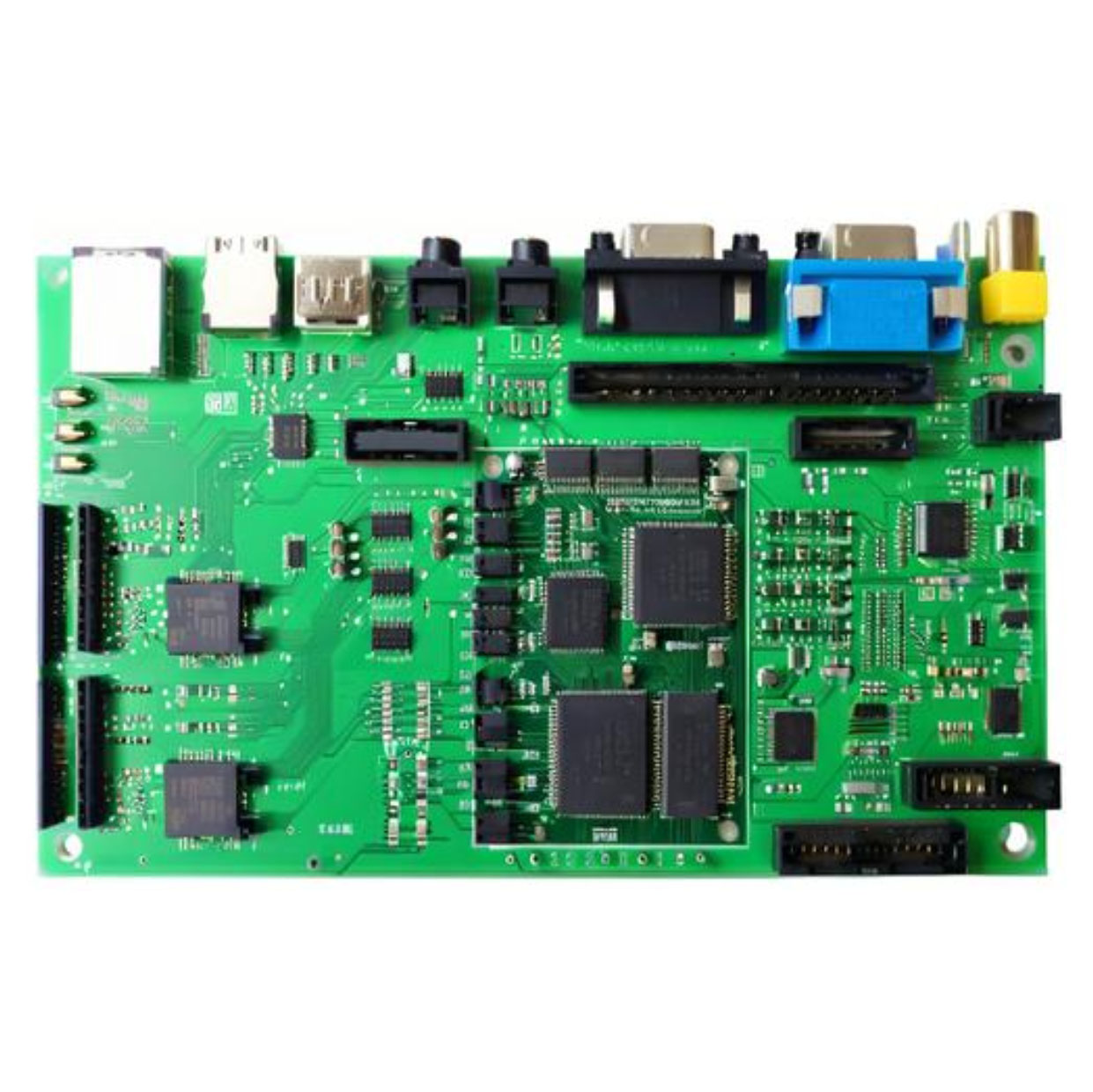
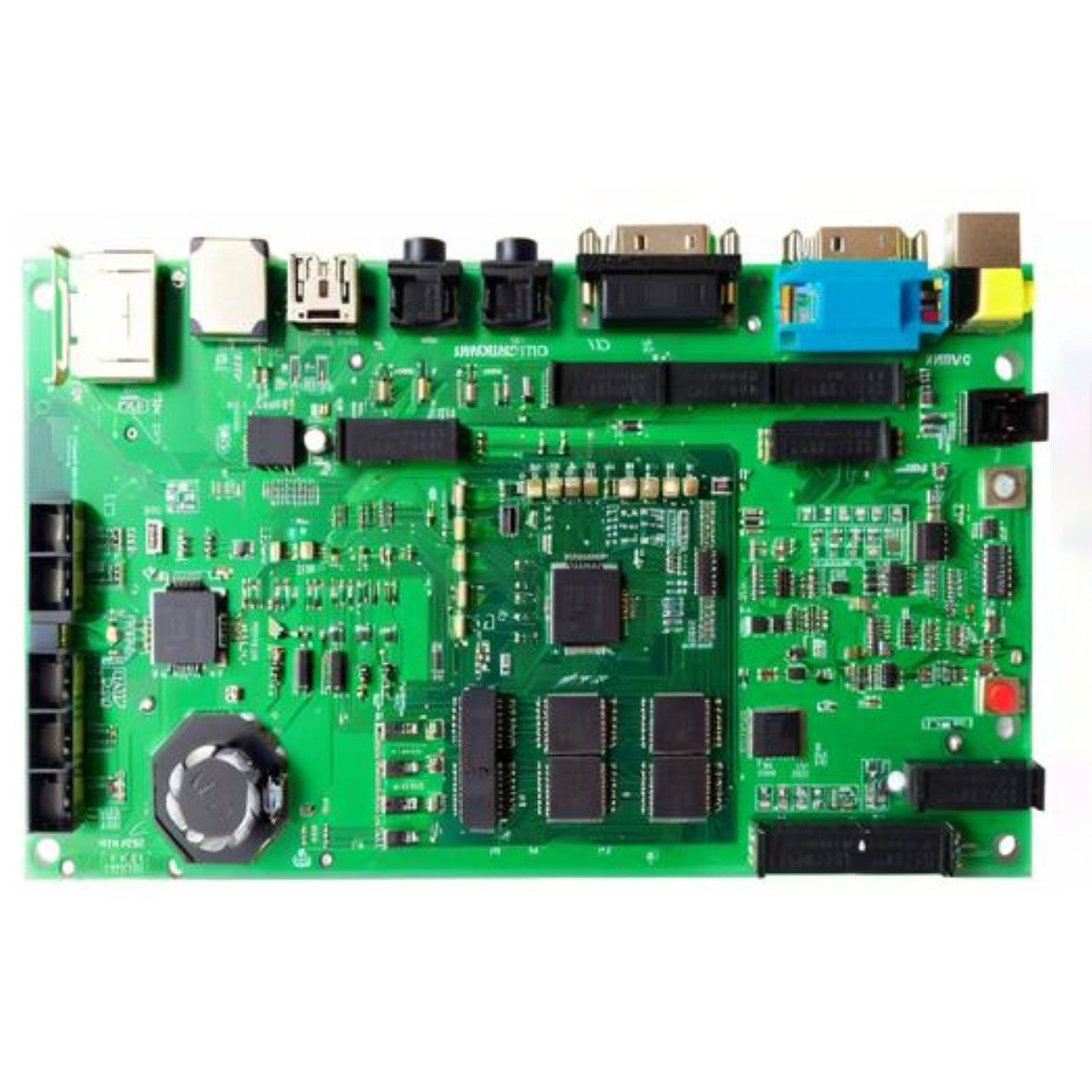
Unlock unbeatable value with our One Stop Electronic OEM PCB Circuit Board Soldering Service-where instant savings and hot deals meet invincible engineering prowess! Famed for enviable quality and innovation, we offer turnkey solutions from custom embedded firmware to PCB design, prototyping, and mass production-up to 100,000 units monthly. Benefit from full BOM procurement, RoHS compliance, and lightning-fast lead times of just 5-15 days. Flexible in color, specification, and connectivity, our all-in-one offer ensures reliable results for every smart device development need.
Precision Materials, Broad Application & Commercial Versatility
Our service employs top-tier base materials such as FR-4, aluminum, and specialized CEM laminates, ensuring durability and electrical precision. Designed for commercial, industrial, and smart device applications, our famed PCB solutions adapt seamlessly to single-sided, double-sided, or multilayer requirements. Whether for environmental testing or embedded sensors, our invincible design capabilities deliver enviable reliability and adaptability, making them ideal for use in consumer electronics, industrial automation, and IoT-enabled technologies.
Swift Payment, Global Export Reach & Efficient Delivery
Enjoy flexible payment terms tailored for commercial buyers alongside express shipping and quick dispatch services. We proudly export to major markets worldwide including the United States, Europe, and Asia, positioning India as the start point of competitive technology excellence. FOB ports are conveniently located for streamlined logistics, ensuring hot deals and reliable export market access for clients seeking to stay ahead with instant savings and swift international deliveries.
FAQ's of One Stop Electronic OEM PCB Circuit Board Soldering Service Smart Devices Firmware Development and PCB Design:
Q: How does your turnkey PCB assembly process function?
A: Our turnkey PCB assembly covers all stages-from component sourcing through production to final testing. Clients submit design files; we handle procurement, assembly, quality testing (including AOI and functional tests), and delivery. Partial turnkey and consignment models are also available.Q: What makes your PCB services enviable for smart device firms?
A: By integrating custom firmware development, environmental testing, and support for varied connectivity standards (USB, Wi-Fi, Bluetooth), our solution creates an invincible platform for smart devices-reducing time-to-market and ensuring famed quality control at every step.Q: When can I expect my completed PCBs after ordering?
A: Depending on your order size and complexity, lead times range from 5 to 15 days. Express shipping and quick dispatch services are available for urgent timelines, ensuring hot deals don't keep you waiting.Q: Where are your PCBs manufactured and exported from?
A: All production takes place in India, equipped with state-of-the-art facilities. We export globally, catering to clients in the USA, Europe, Asia, and beyond, with efficient logistics through local FOB ports.Q: What benefits do I gain from your prototyping and mass production services?
A: You receive a streamlined process-from design through full-volume manufacturing-using famed design software, robust materials, and environmental testing. Plus, our flexible options and instant savings offer unmatched commercial value for any electronic application.Tell us about your requirement

Price:
Quantity
Select Unit
- 50
- 100
- 200
- 250
- 500
- 1000+
Additional detail
Mobile number
Email

Other Products in 'PCBA Customized' category
Contact Details
- No. 1506,15 Floor, SSG Tower, 561 ADien Bien Phu Str, Ward 25, Binh Thanh Dist, HCMC, Ho Chi Minh City - 717000, Thanh Pho Ho Chi Minh, Vietnam
- Ms. Yolanda Ke (Sales Account Manager)
- Mobile : +8613751081371
- Send Inquiry
NOVA TECHNOLOGY VIETNAMESE COMPANY LIMITED
|
 Call Me Free

NOVA TECHNOLOGY VIETNAMESE COMPANY LIMITED
All Rights Reserved.(Terms of Use)
Developed and Managed by Infocom Network Private Limited.
Developed and Managed by Infocom Network Private Limited.
