


China Custom Smart Electronic PCBA Manufacturer OEM Fabrication PCB Prototype supplier
Product Details:
- Silkscreen White
- Impedance Controlled
- Insulation Resistance >10^12
- Min. Line Width 0.1 mm
- Soldermask Green
- Board Type Rigid/Custom
- Voltage Endurance 1500V
- Click to view more
X
China Custom Smart Electronic PCBA Manufacturer OEM Fabrication PCB Prototype supplier Price And Quantity
- INR
- 1
- One-stop SMT & DIP assembly
- Consumer Electronics, Smart Devices, IoT
- Green, Red, Blue, Black, White
- ESD Packaging/Anti-Static Bag
- Full Turnkey or Partial Kit
- SMT and THT Supported
- 7-15 days prototype
- Automated Optical Inspection, X-ray
- Custom OEM/ODM
- China
China Custom Smart Electronic PCBA Manufacturer OEM Fabrication PCB Prototype supplier Product Specifications
- 0.2 mm (Min)
- Green
- 1 oz - 2 oz
- Available
- SMT & Through Hole
- 0.1 mm
- 0.1 mm
- Green
- Rigid/Custom
- Custom
- White
- Controlled
- >10^12
- 100% E-Test, AOI
- 1500V
- HASL, ENIG
- 2-12 Layers
- 1.6 mm
- FR-4
- UL94V-0
- Smart Electronic PCBA
- One-stop SMT & DIP assembly
- Consumer Electronics, Smart Devices, IoT
- Green, Red, Blue, Black, White
- ESD Packaging/Anti-Static Bag
- Full Turnkey or Partial Kit
- SMT and THT Supported
- 7-15 days prototype
- Automated Optical Inspection, X-ray
- Custom OEM/ODM
- China
Product Description
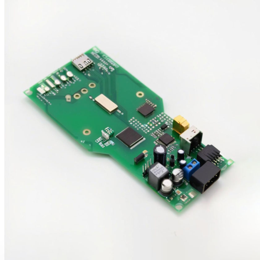
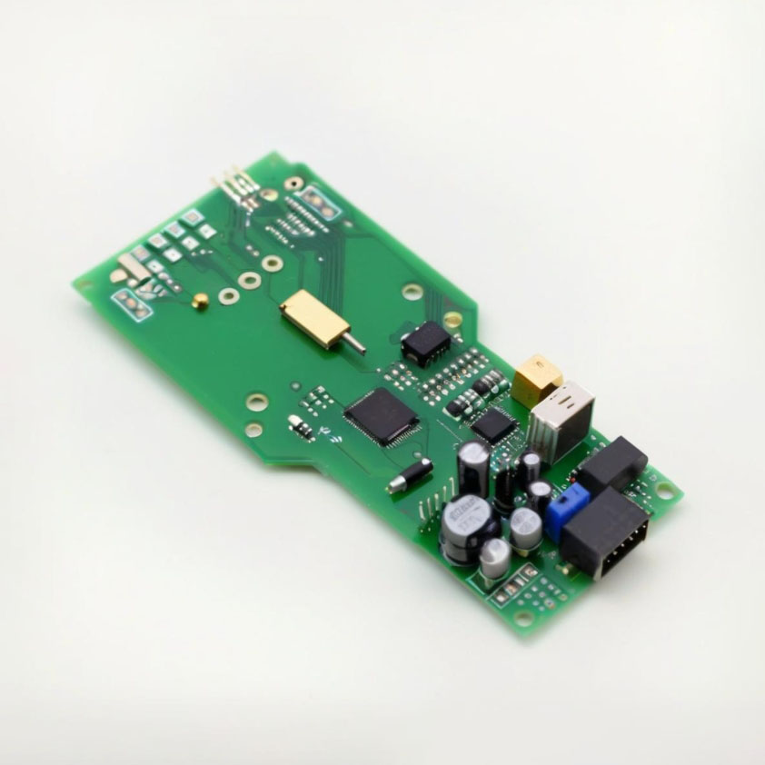
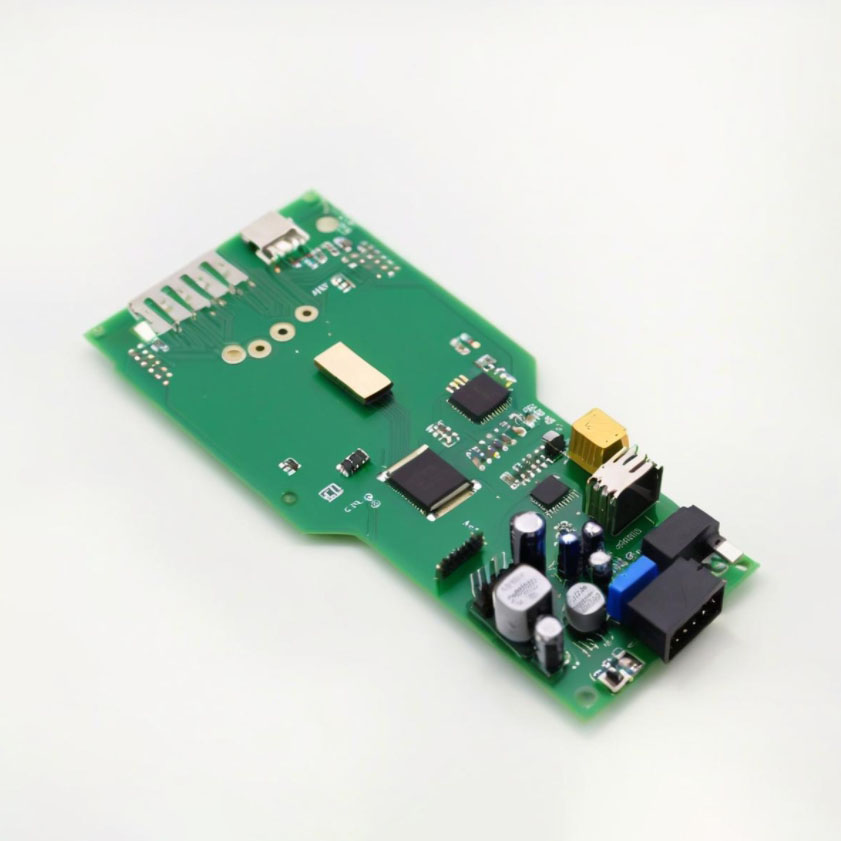
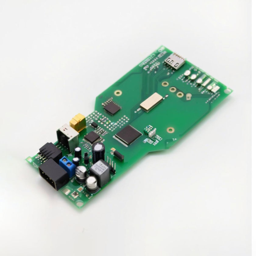
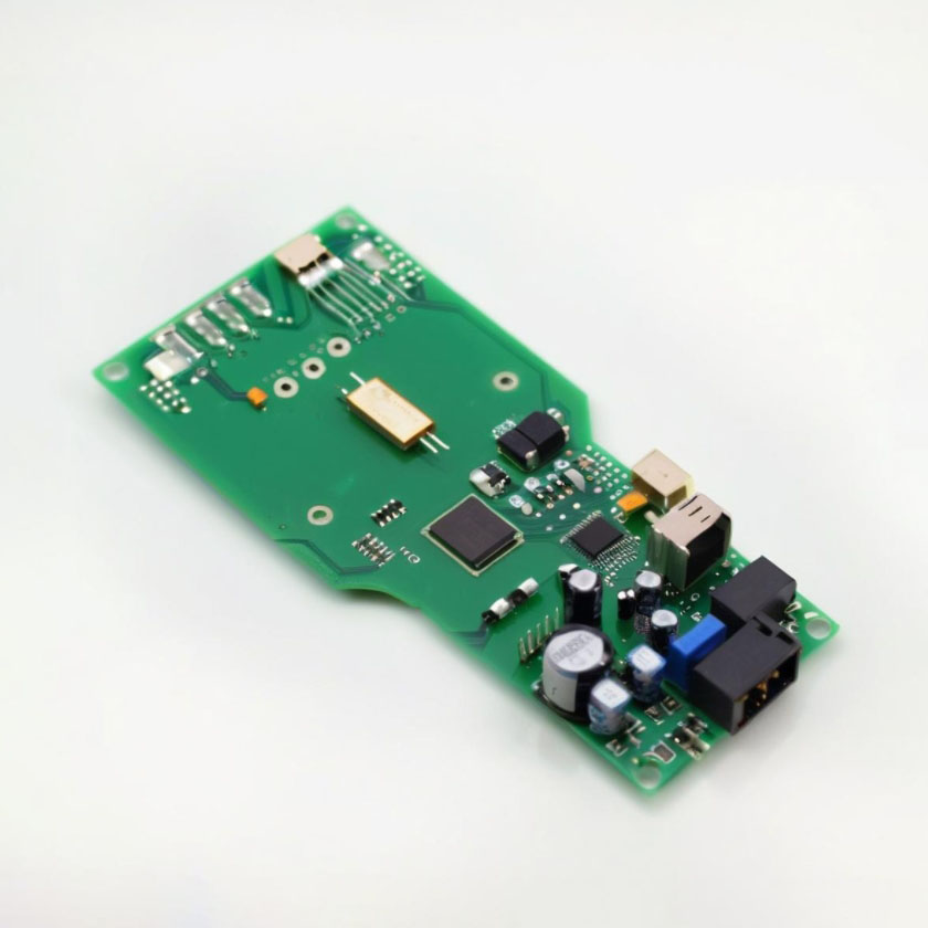
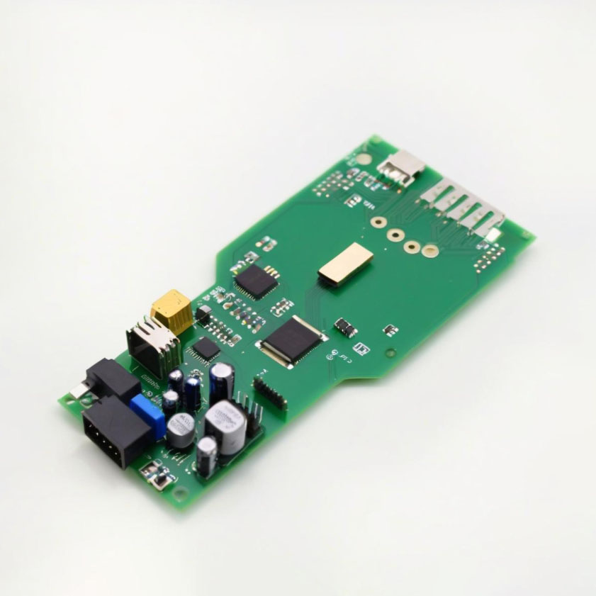
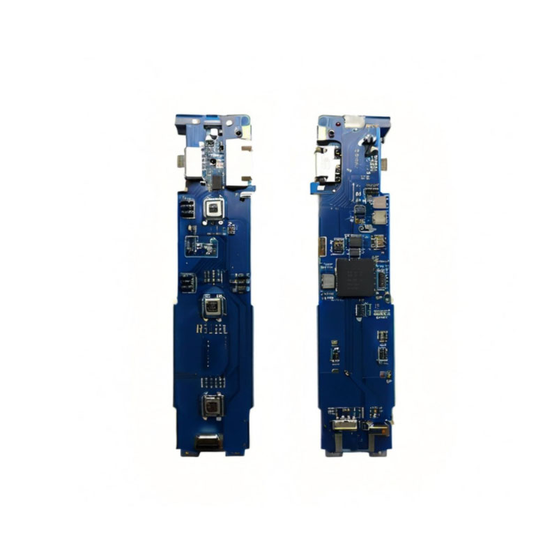
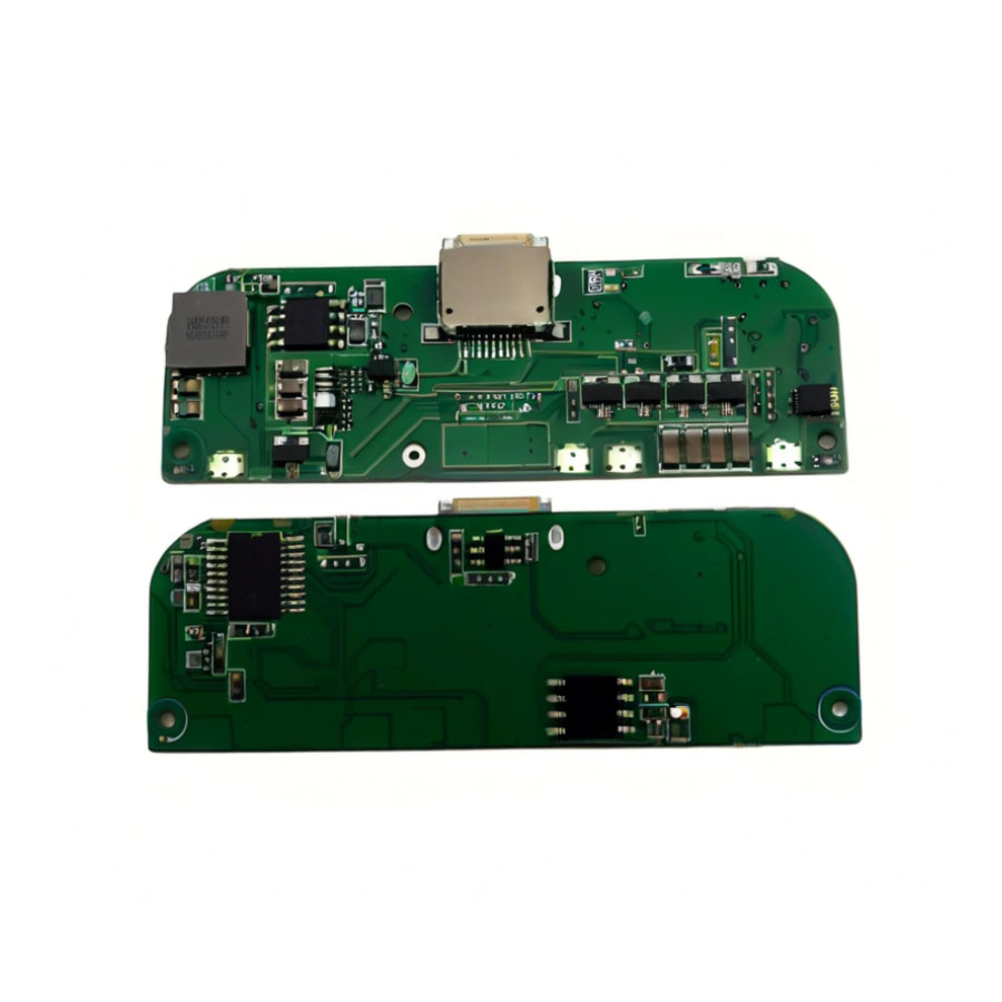
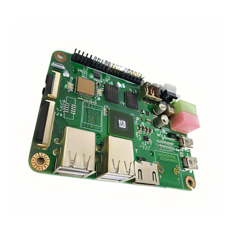
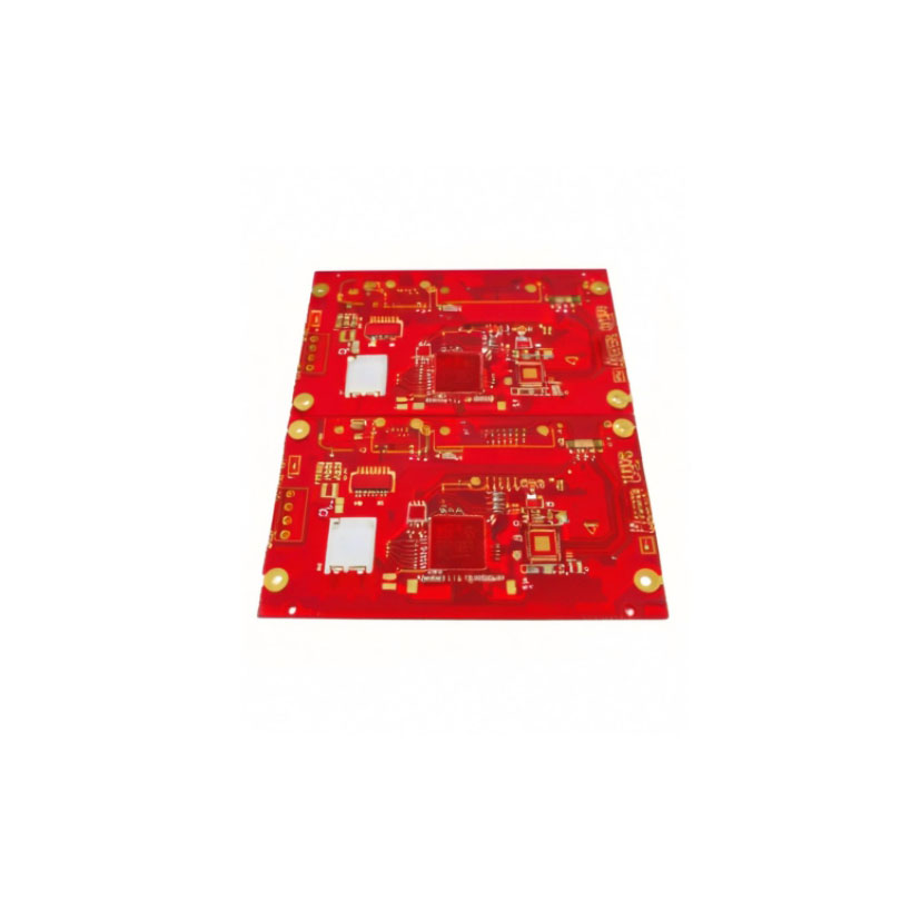
Scarce in the industry for such versatility, our China Custom Smart Electronic PCBA Manufacturer is highly recommended by professionals worldwide. Boasting favorable reviews, this champion supplier offers enlightened solutions for OEM fabrication and intelligent PCB prototypes, establishing new benchmarks of opulence in electronics manufacturing. Customizable dimensions, one-stop SMT & DIP assembly, UL94V-0 flame resistance, and advanced testing including AOI and X-ray ensure impeccable reliability. Full turnkey component sourcing and rapid 7-15 day lead times make this service a coveted asset in smart devices, IoT, and consumer electronics.
Versatility Redefined: Applications & Features
Our smart electronic PCBAs are extensively used for consumer electronics, smart devices, and comprehensive IoT applications. They champion adaptation with custom OEM/ODM dimensions and multi-layer support (2-12 layers), including sensor switch integration. These PCBs offer extra features like controlled impedance, robust voltage endurance, and opulent silk screening options. Rigorous quality control (AOI, X-ray) and flexible mounting technology (SMT & THT) make them ideal for large-scale plant applications, ensuring superior operational integrity.
Swift Delivery & Flexible Payment Terms
Expect your orders to be shipped promptly, with standard delivery times ranging from 7 to 15 days for prototypes. Packaging is secure with ESD/anti-static options ensuring optimum protection. We maintain clear sample policies to ease initial bulk ordering. The asking price is tailored to the custom solution needed and payment terms are adaptable, offering flexibility for international buyers. Our streamlined processes ensure each product reaches you safely and efficiently, supporting smooth business transactions.
FAQ's of China Custom Smart Electronic PCBA Manufacturer OEM Fabrication PCB Prototype supplier:
Q: How does the custom PCBA manufacturing process work?
A: The process begins with your custom design or OEM/ODM requirements, followed by precise SMT and DIP assembly. Advanced testing methods such as 100% E-Test, Automated Optical Inspection (AOI), and X-ray are used to guarantee quality before secure ESD packaging and global shipment.Q: What unique features set this PCBA supplier apart?
A: Our PCBA solutions provide controlled impedance, UL94V-0 flame resistance, comprehensive component sourcing (full turnkey or partial kit), and multi-color solder mask options. With custom panel sizes, sensor switches, and integration of both SMT and through-hole technology, we offer exceptional adaptability and quality control.Q: When can I expect my prototype to be delivered?
A: Typically, prototypes are shipped within 7 to 15 days after confirming the order, depending on the complexity and order volume.Q: Where are the materials for the PCBAs sourced from?
A: All base materials are sourced directly from China, ensuring reliable quality and compliance with international standards for consumer electronics and smart device applications.Q: What benefits do automated inspections provide?
A: Automated Optical Inspection (AOI) and X-ray testing significantly reduce defects, enhance product reliability, and assure that each batch meets stringent quality standards before leaving our facility.Tell us about your requirement

Price:
Quantity
Select Unit
- 50
- 100
- 200
- 250
- 500
- 1000+
Additional detail
Mobile number
Email

Other Products in 'PCBA Customized' category
Contact Details
- No. 1506,15 Floor, SSG Tower, 561 ADien Bien Phu Str, Ward 25, Binh Thanh Dist, HCMC, Ho Chi Minh City - 717000, Thanh Pho Ho Chi Minh, Vietnam
- Ms. Yolanda Ke (Sales Account Manager)
- Mobile : +8613751081371
- Send Inquiry
NOVA TECHNOLOGY VIETNAMESE COMPANY LIMITED
|
 Call Me Free

NOVA TECHNOLOGY VIETNAMESE COMPANY LIMITED
All Rights Reserved.(Terms of Use)
Developed and Managed by Infocom Network Private Limited.
Developed and Managed by Infocom Network Private Limited.
