


Professional Engineer one stop Rapid Schematic Electronic Pcb Design And Software Manufacturer
Product Details:
- Voltage Endurance 1500V AC
- Flame Resistance Level UL 94V-0
- Silkscreen White, Yellow, Black
- Min. Line Spacing 0.075mm (3mil)
- Min. Line Width 0.075mm (3mil)
- Board Type Rigid, Flexible, Rigid-Flex
- Test 100% E-test & Visual Inspection
- Click to view more
X
Professional Engineer one stop Rapid Schematic Electronic Pcb Design And Software Manufacturer Price And Quantity
- INR
- 1
- Yes
- Turnkey BOM, Partial, Consignment
- Altium Designer, Eagle, OrCAD, KiCAD, PADS
- DHL, FedEx, UPS, Air, Sea
- Vacuum and ESD-safe packing
- Engineering and technical consultation
- 24h-48h for samples
- SMT, DIP, Mixed, BGA, Fine Pitch
- Up to 30,000 sq.m/month
Professional Engineer one stop Rapid Schematic Electronic Pcb Design And Software Manufacturer Product Specifications
- UL 94V-0
- 1500V AC
- HASL, ENIG, OSP, Immersion Silver/Tin, Gold Plating
- Professional Engineer One Stop Rapid Schematic Electronic PCB Design And Software Manufacturer
- 0.075mm (3mil)
- 1.6mm (customizable)
- FR4, CEM-1, CEM-3, Rogers, Aluminum, Flex
- 10% Controlled Impedance
- Rigid, Flexible, Rigid-Flex
- Min. 0.2mm
- Green (custom options available)
- 0.075mm (3mil)
- White, Yellow, Black
- Single, Double, Multilayer up to 18L
- >500V DC
- Integrated options available upon request
- Standard 18 x 24 (custom size available)
- 1oz / 2oz (customizable)
- SMD, Through-hole, Mixed Mounting
- Green, Red, Blue, Black, Yellow, White
- 100% E-test & Visual Inspection
- Yes
- Turnkey BOM, Partial, Consignment
- Altium Designer, Eagle, OrCAD, KiCAD, PADS
- DHL, FedEx, UPS, Air, Sea
- Vacuum and ESD-safe packing
- Engineering and technical consultation
- 24h-48h for samples
- SMT, DIP, Mixed, BGA, Fine Pitch
- Up to 30,000 sq.m/month
Product Description
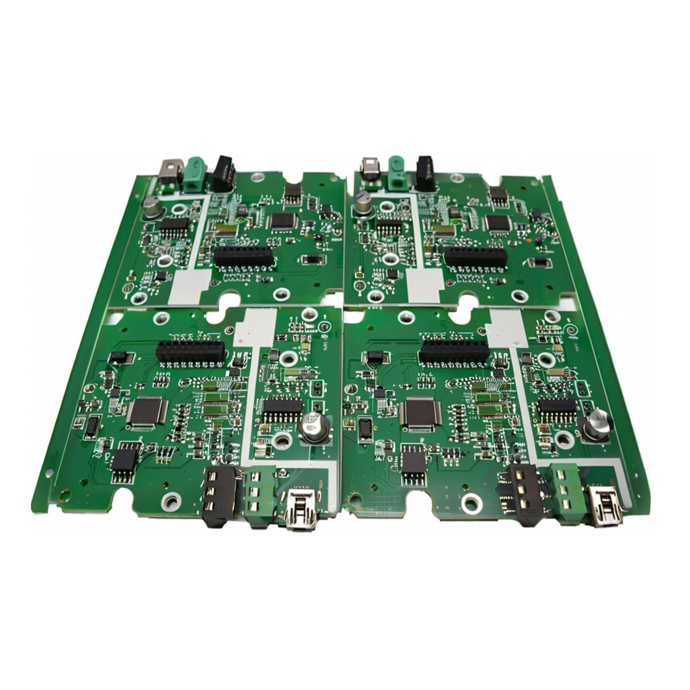
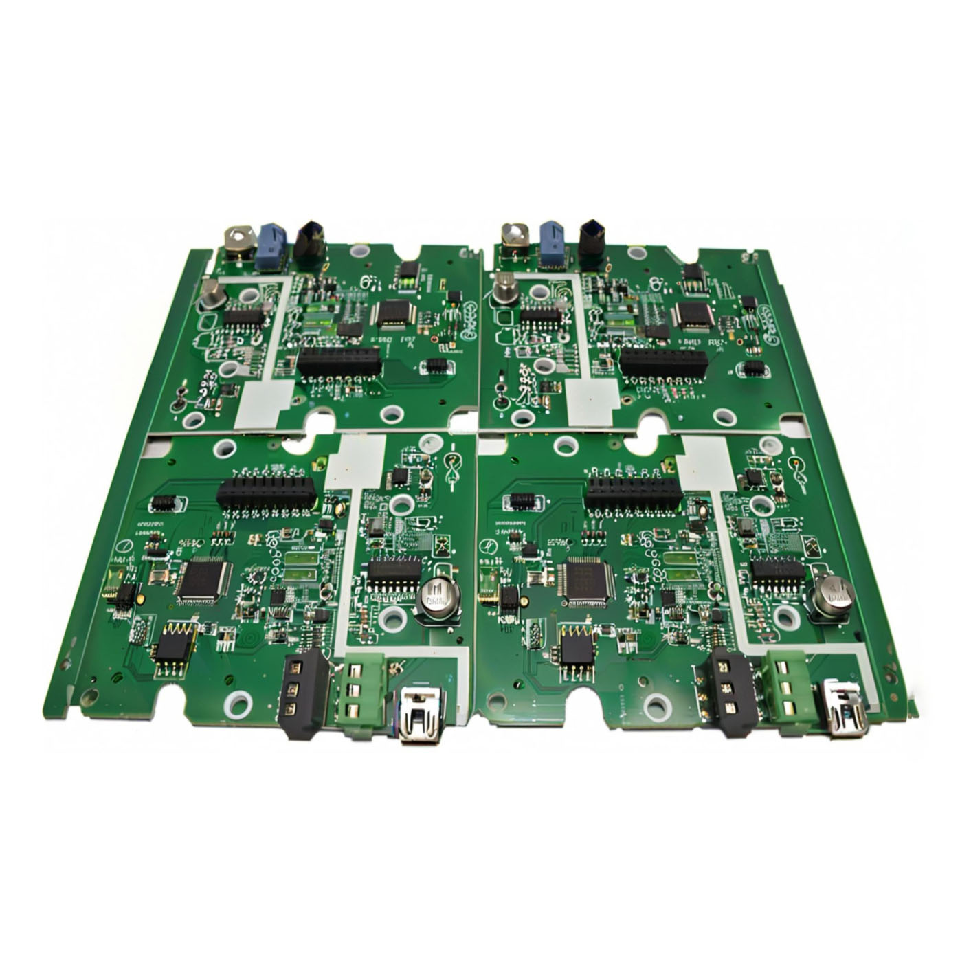
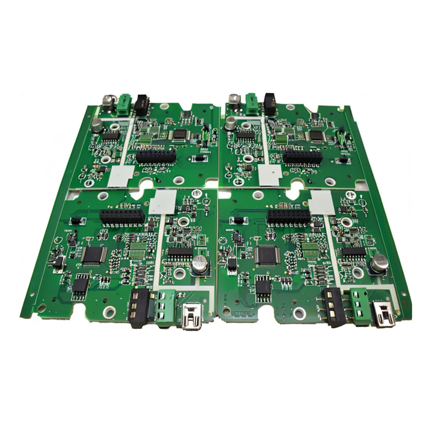
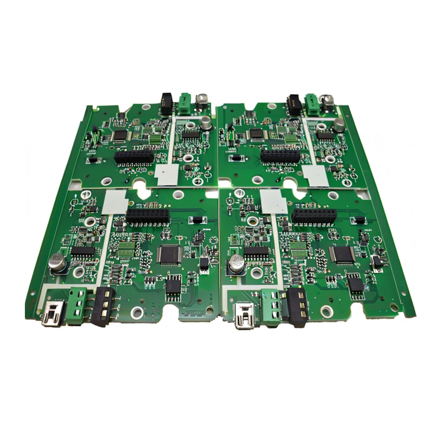
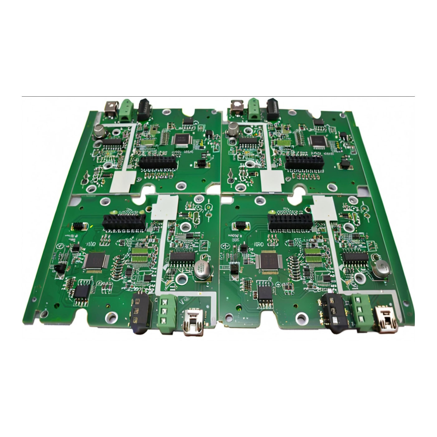
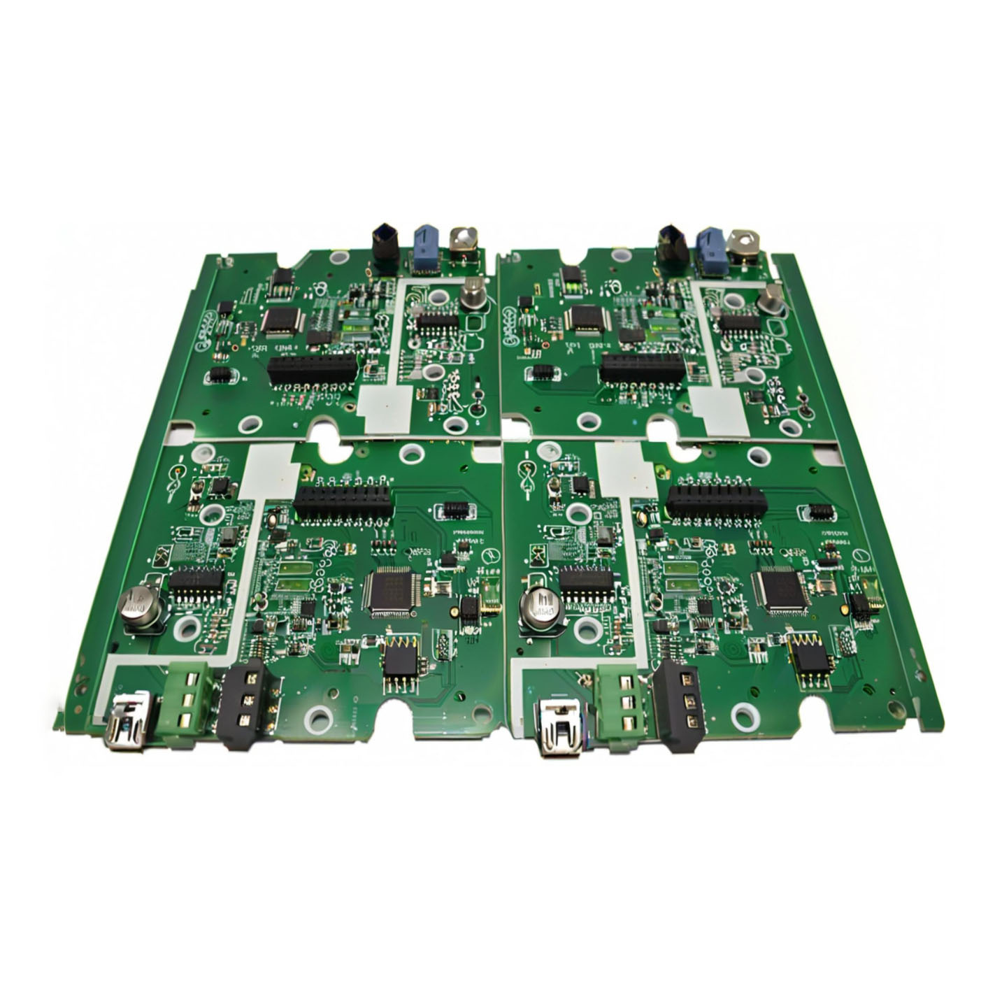
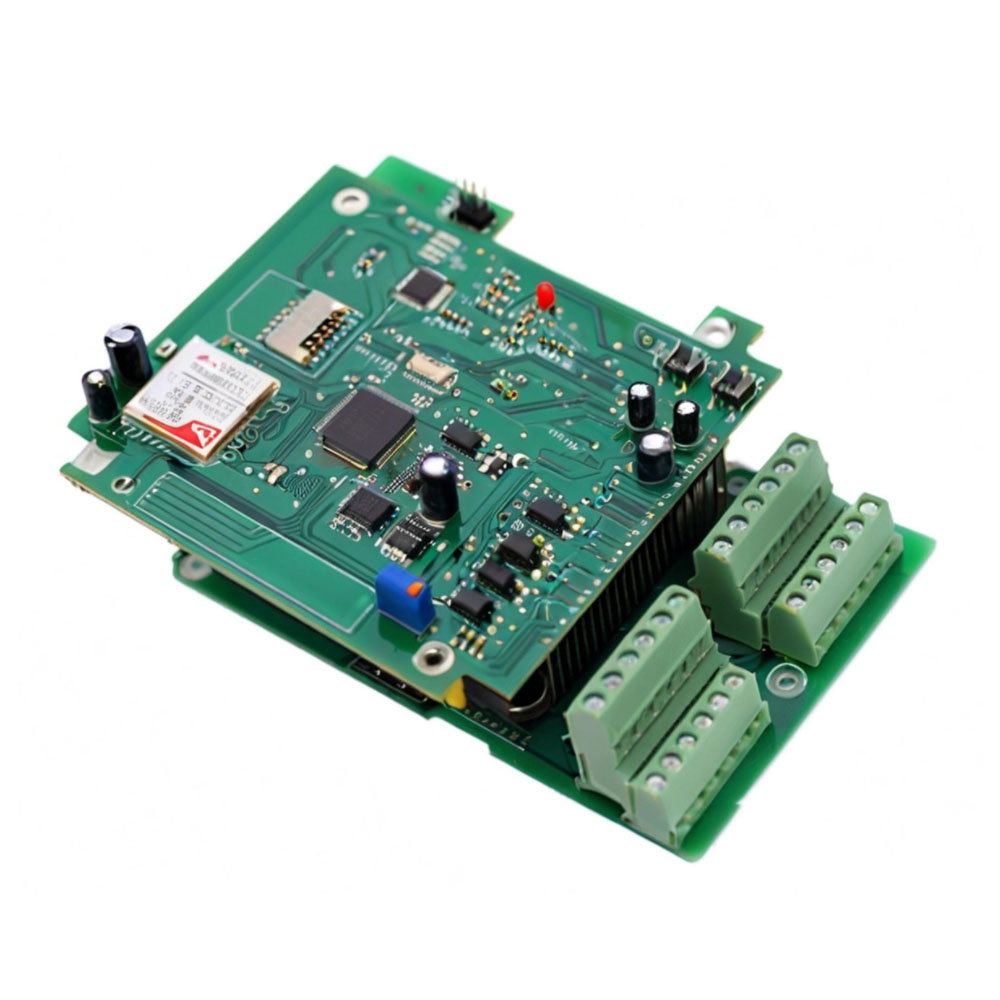
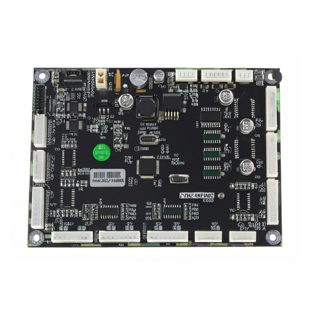
Get commanding results with our marvelous Professional Engineer one stop Rapid Schematic Electronic PCB Design and Software Manufacturing services-a must-have for innovative engineers and technology businesses. Harness the valiant support of leading design platforms like Altium Designer, Eagle, OrCAD, KiCAD, and PADS to accelerate your project with rapid prototyping (24-48h) and robust monthly production up to 30,000 sq.m. Enjoy impressive savings without compromise on quality, thanks to RoHS compliance, turnkey BOM sourcing, and advanced assembly options-SMT, DIP, BGA, and more. Secure, ESD-safe packaging and global shipping ensure timely delivery. Get after-sales engineering support for seamless project completion.
Versatile Applications & Key Features
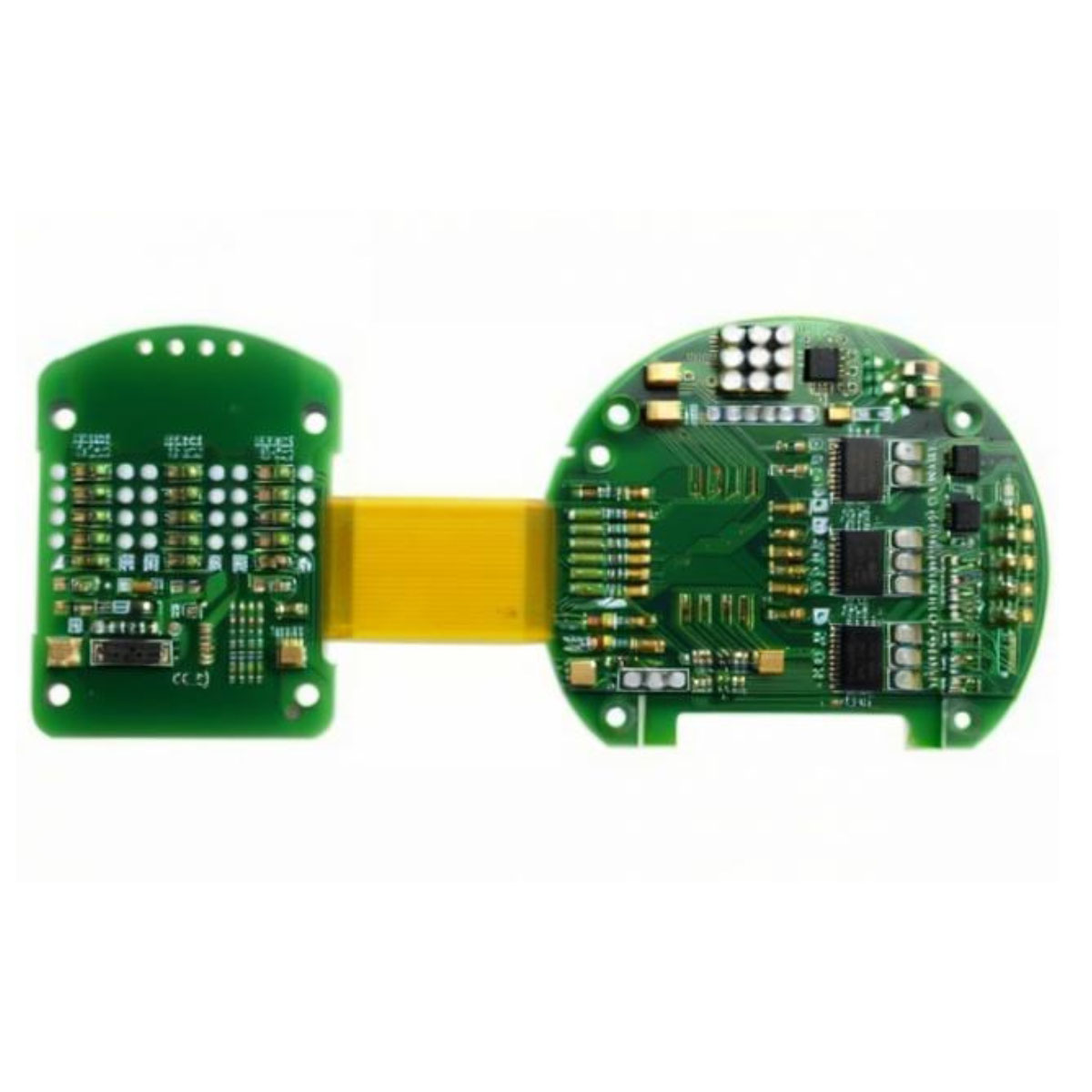
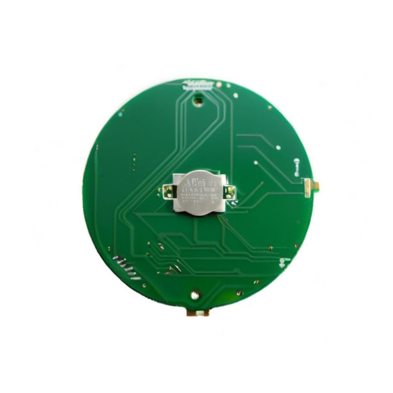
This PCB design and software manufacturing service is ideal for electronics, automotive, medical, and industrial automation sectors, integrating sensor switch options and mixed mounting techniques for both prototyping and mass production. Its broad application scope includes consumer appliances, IoT devices, and communication equipment. Feature-rich with customizable layer counts, sizes, soldermask colors, and board types-rigid, flexible, or rigid-flex-you receive dependable solutions with 100% E-test verification and RoHS-compliant construction.
Payment Terms, Export Markets, and Sample Rates
Enjoy competitive rates and hassle-free order completion, with payment terms suited for global clients. Serving main export markets such as USA, Europe, Asia, and the Middle East, we guarantee efficient logistics through DHL, FedEx, UPS, air, or sea transport. Sample PCBs are available for evaluation at attractive terms, ensuring confidence before large-scale orders. Our dedicated logistics team ensures prompt shipping, order tracking, and reliable delivery to your location worldwide.
Versatile Applications & Key Features
This PCB design and software manufacturing service is ideal for electronics, automotive, medical, and industrial automation sectors, integrating sensor switch options and mixed mounting techniques for both prototyping and mass production. Its broad application scope includes consumer appliances, IoT devices, and communication equipment. Feature-rich with customizable layer counts, sizes, soldermask colors, and board types-rigid, flexible, or rigid-flex-you receive dependable solutions with 100% E-test verification and RoHS-compliant construction.
Payment Terms, Export Markets, and Sample Rates
Enjoy competitive rates and hassle-free order completion, with payment terms suited for global clients. Serving main export markets such as USA, Europe, Asia, and the Middle East, we guarantee efficient logistics through DHL, FedEx, UPS, air, or sea transport. Sample PCBs are available for evaluation at attractive terms, ensuring confidence before large-scale orders. Our dedicated logistics team ensures prompt shipping, order tracking, and reliable delivery to your location worldwide.
FAQ's of Professional Engineer one stop Rapid Schematic Electronic Pcb Design And Software Manufacturer:
Q: How do I initiate the PCB design and manufacturing process with your company?
A: Simply submit your design files and project requirements through our online portal or email, specifying your preferred software platform, board specifications, and assembly needs. Our engineers will promptly review and confirm all details with you.Q: What are the advantages of using your Professional Engineer one stop solution?
A: Our all-in-one solution streamlines PCB design, prototyping, and production, reducing time, costs, and coordination efforts. Full design software support, rapid turnaround, component sourcing, and after-sales technical consultation make it a convenient option for engineers and product developers.Q: Where do you export your PCBs, and what are the main markets you serve?
A: We export to various regions, with primary markets in the USA, Europe, Asia, and the Middle East, catering to a wide range of industry verticals and business sizes.Q: When can I expect the prototyping samples to be ready for review?
A: Prototyping samples are typically prepared within 24 to 48 hours after finalizing design approval and material confirmation, ensuring a rapid start to your project.Q: What are the different assembly and packaging options available?
A: We offer SMT, DIP, mixed, BGA, and fine-pitch assembly, with packaging that includes vacuum sealing, ESD-safe materials, and customizable shipping arrangements to protect and expedite your orders.Q: How does your after-sales support benefit my engineering team?
A: Our after-sales support includes engineering and technical consultation, helping you address design challenges, resolve production issues, and optimize performance for ongoing or future PCB projects.Tell us about your requirement

Price:
Quantity
Select Unit
- 50
- 100
- 200
- 250
- 500
- 1000+
Additional detail
Mobile number
Email

Other Products in 'PCBA Customized' category
Contact Details
- No. 1506,15 Floor, SSG Tower, 561 ADien Bien Phu Str, Ward 25, Binh Thanh Dist, HCMC, Ho Chi Minh City - 717000, Thanh Pho Ho Chi Minh, Vietnam
- Ms. Yolanda Ke (Sales Account Manager)
- Mobile : +8613751081371
- Send Inquiry
NOVA TECHNOLOGY VIETNAMESE COMPANY LIMITED
|


NOVA TECHNOLOGY VIETNAMESE COMPANY LIMITED
All Rights Reserved.(Terms of Use)
Developed and Managed by Infocom Network Private Limited.
Developed and Managed by Infocom Network Private Limited.
