Product Description
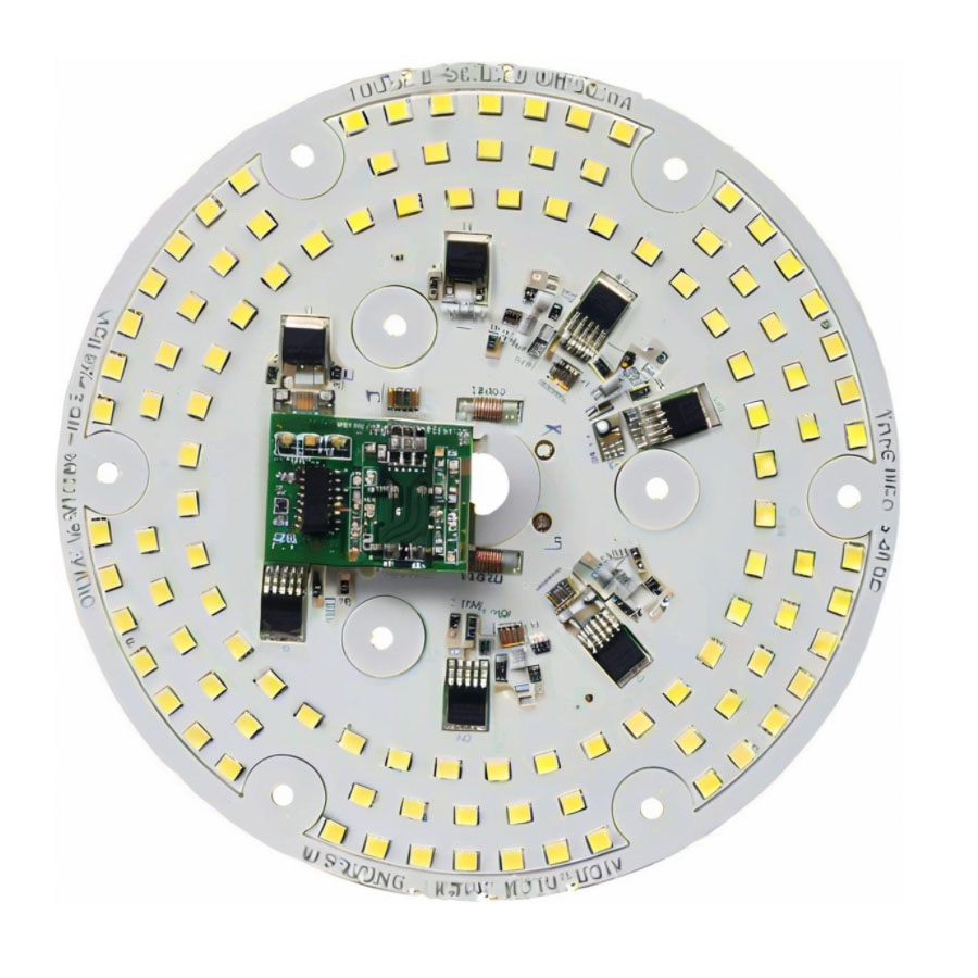
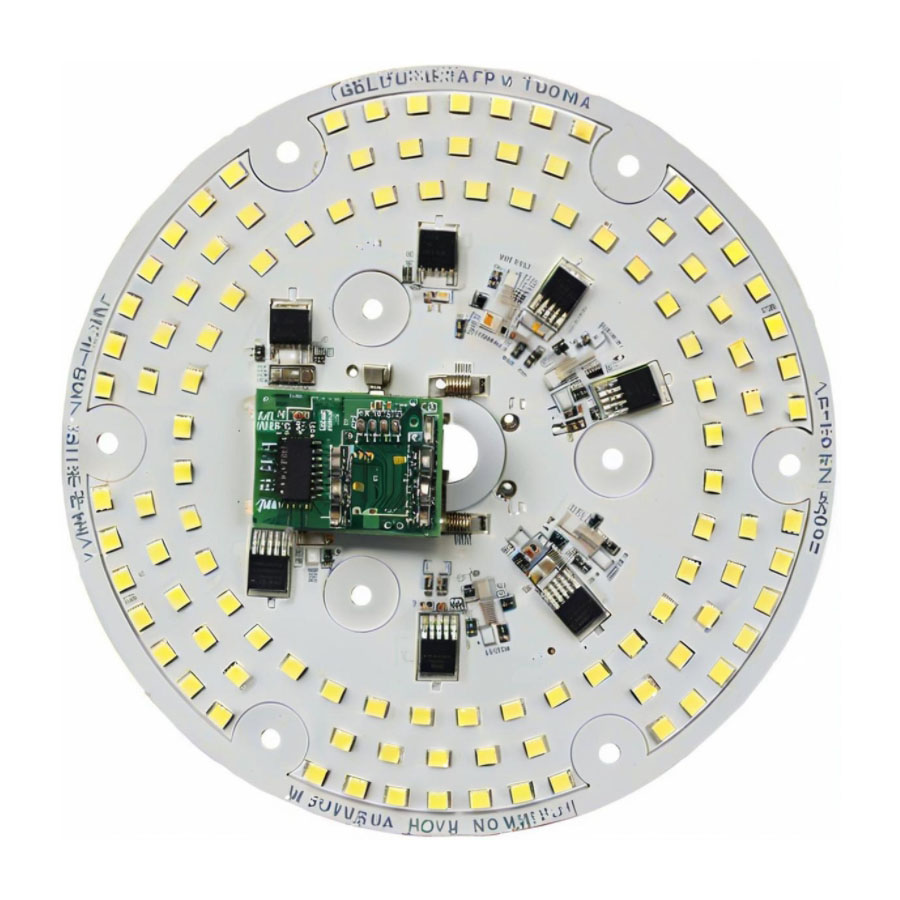
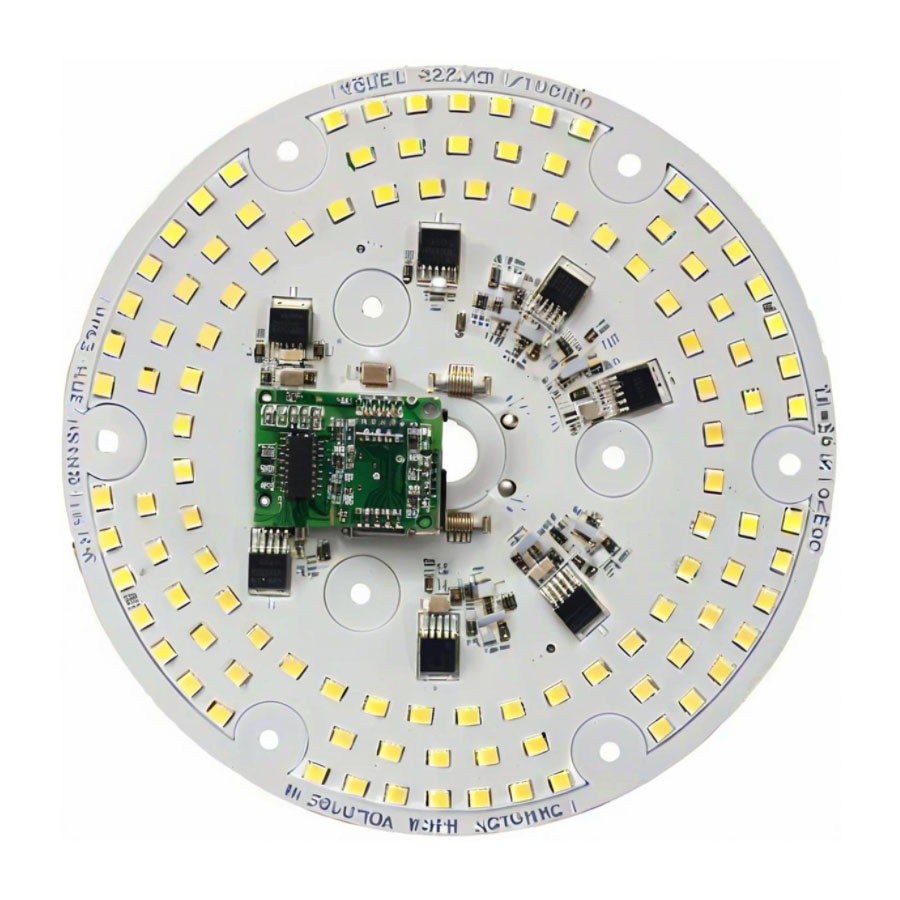
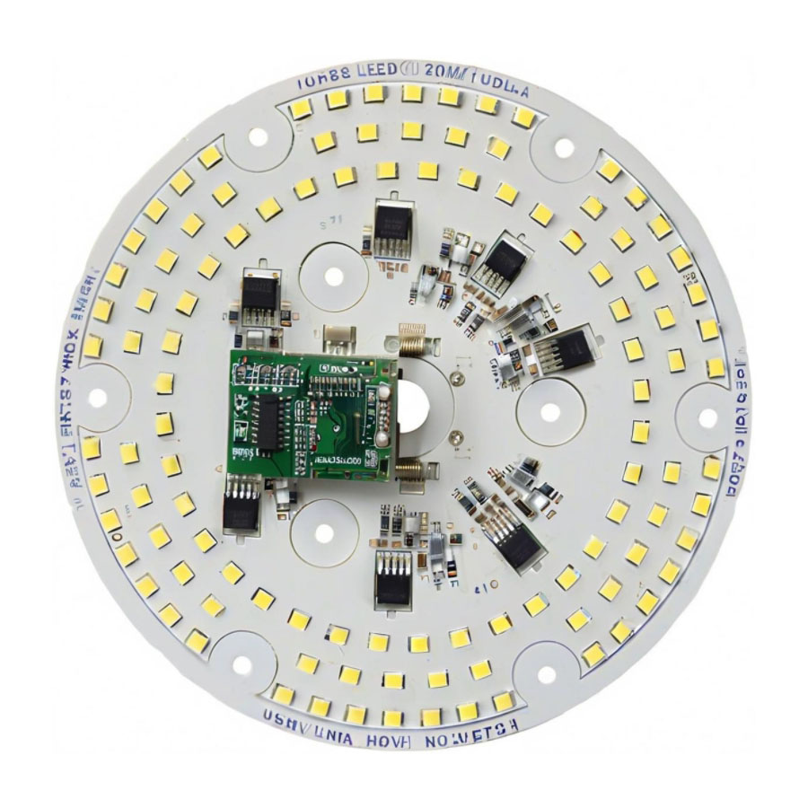
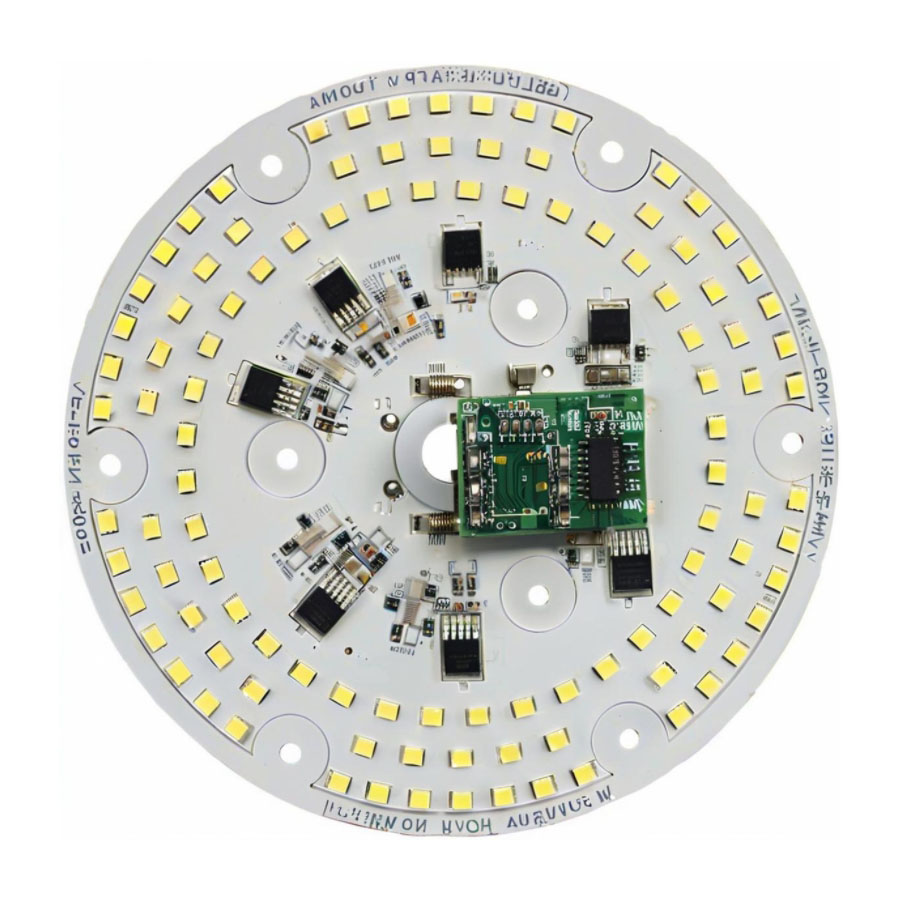
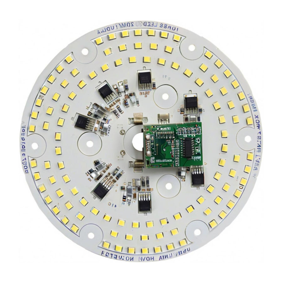
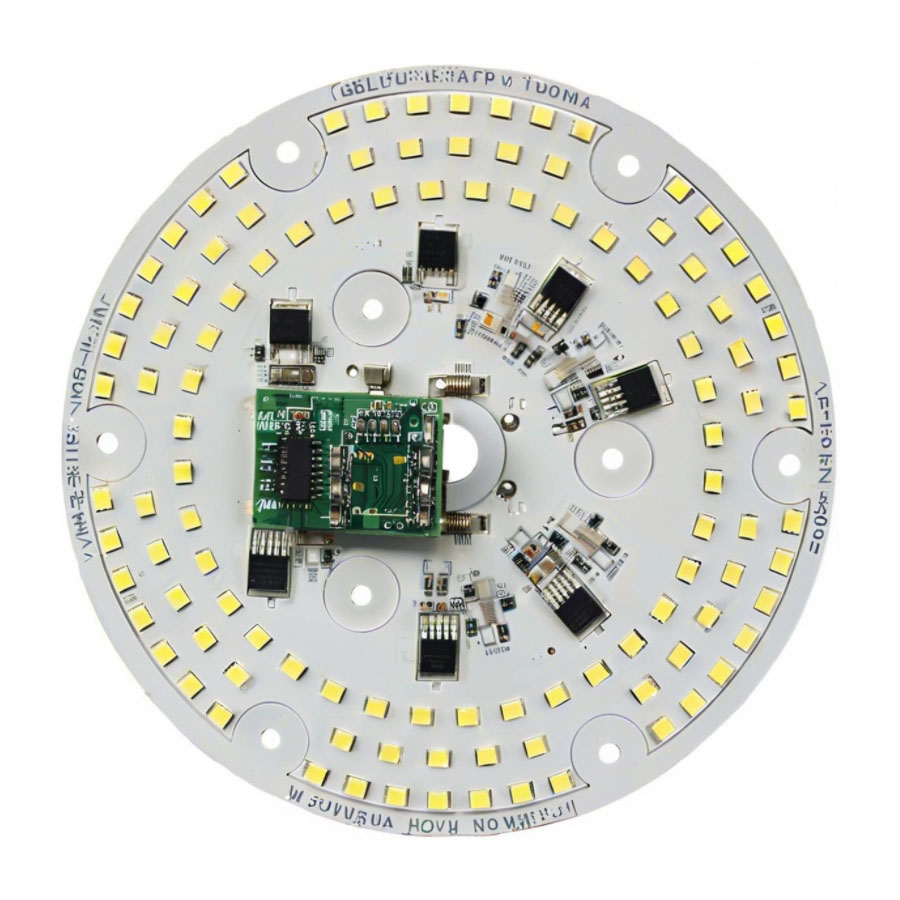
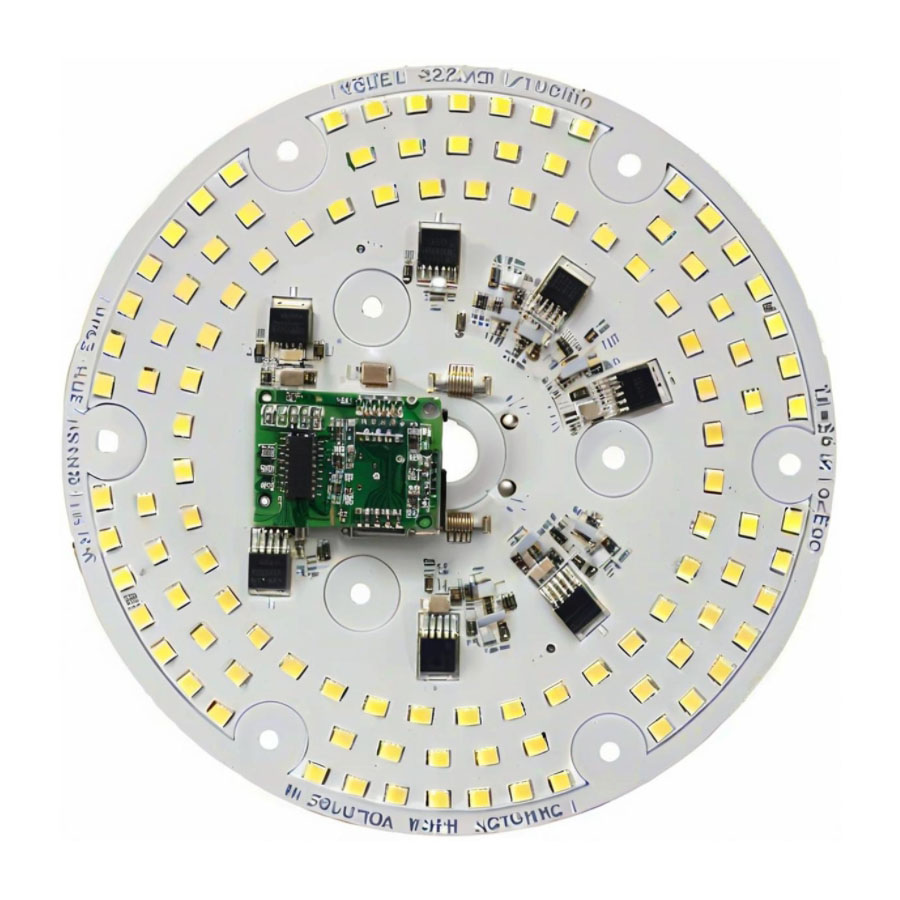
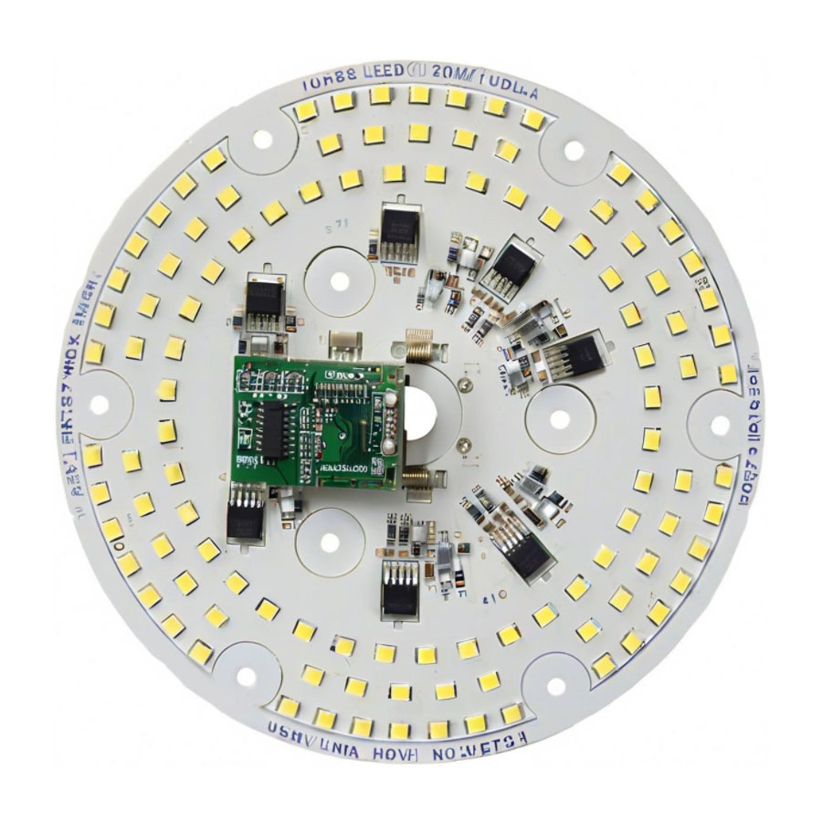
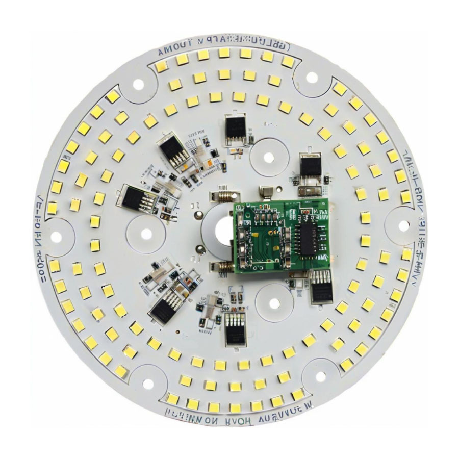
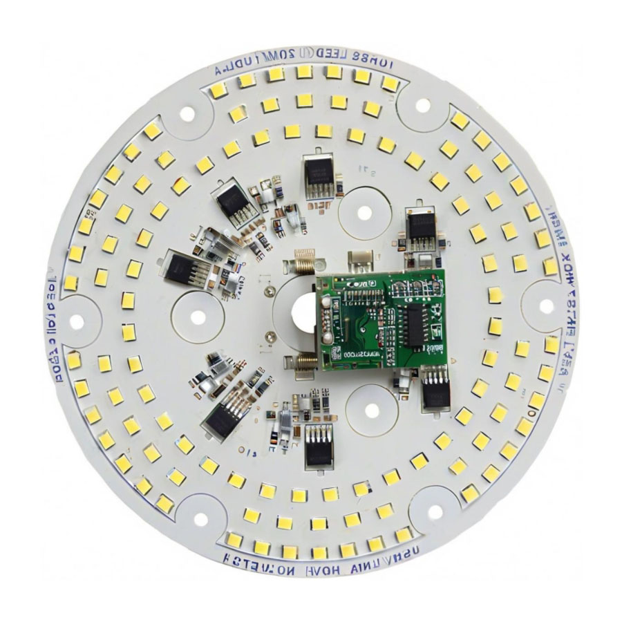
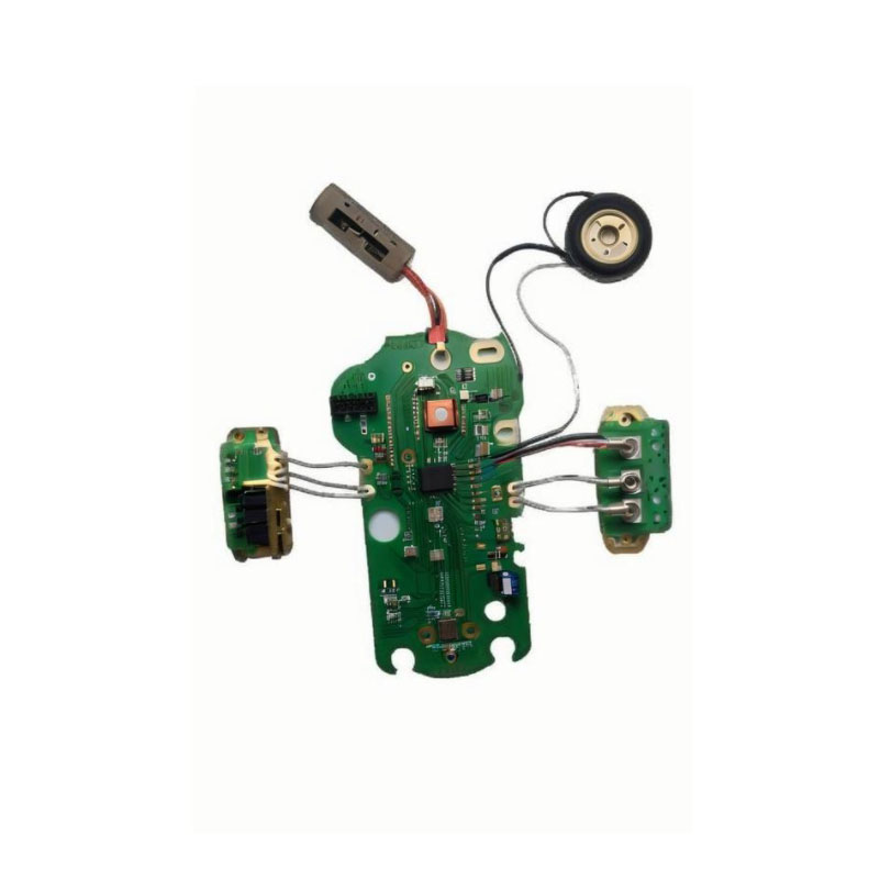
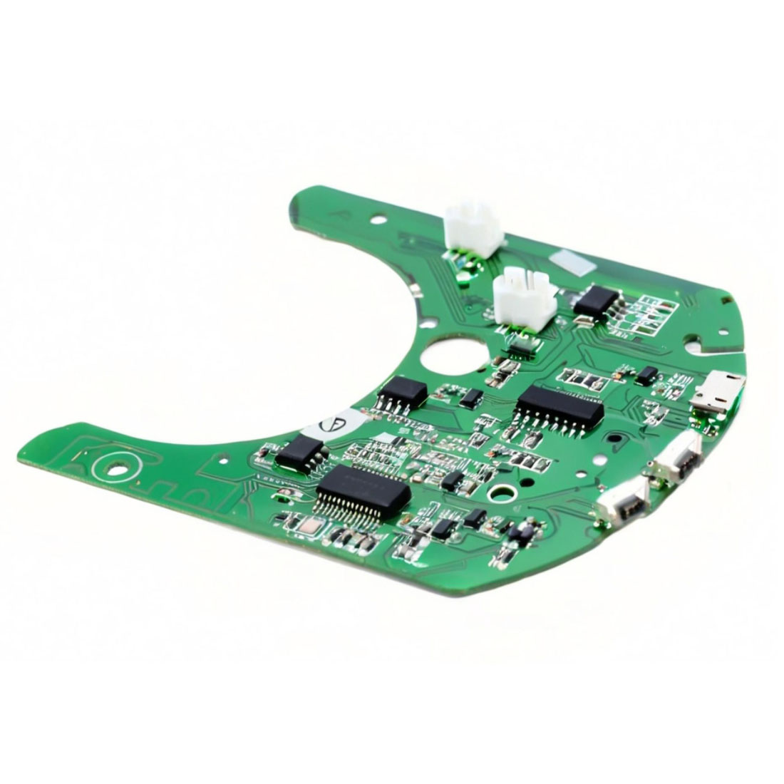
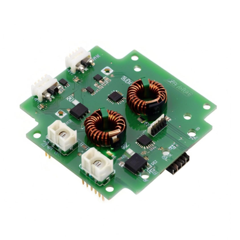
Discover instant savings and reduced prices on our premier Professional Customized PCB Assembly services, with exclusive offers ending soon. As a renowned manufacturer and exporter in India, we provide first-rate, one-stop OEM/ODM solutions for Other PCB & PCBA, including Wireless Charger PCBA assemblies. Our advanced assembly processes-SMT, DIP, and hand soldering-utilize high quality SMD & DIP components, ensuring stable wireless charging performance and reliability. Whether you require full turnkey or partial component sourcing, each project is customized to your specifications, featuring strict ICT, FCT, X-ray, and aging tests. Minimize your costs and streamline your production with our superior packaging, rapid 7-15 day lead times, and flexible MOQs.
Versatile Applications and Superior Usage
Our Professional Customized PCB Assembly and Wireless Charger PCBA are engineered for wide-ranging applications, including consumer electronics, wireless power supply modules, and integrated touch sensor solutions. Designed with flexibility in mind, they support both SMD and DIP mounting for specific usage requirements in devices such as wireless chargers, smart gadgets, and portable electronics. Each product boasts stable performance, ensuring efficient power management and reliable operation across multiple industries.
Swift Delivery, Verified Quality, and FOB Details
Order processing for our PCB Assembly and Wireless Charger PCBA begins immediately, providing a fast estimate on lead times and sale prices. With a typical delivery time of 7 to 15 working days, your project stays on track. Each assembly undergoes full certification and rigorous testing, ensuring top quality. Our standard FOB port options cover major Indian ports, supporting seamless global export and reliable, timely fulfillment of your manufacturing needs.
FAQ's of Professional Customized Pcb Assembly Other PCB&PCBA Pcba Wireless Charger Pcba one stop service Manufacturer:
Q: How does the one-stop OEM/ODM solution benefit my production process?
A: Our one-stop OEM/ODM PCB assembly service streamlines your project by integrating design, sourcing, testing, assembly, and packaging, reducing coordination effort and ensuring high quality at faster turnaround times.
Q: What assembly processes are available for custom PCB production?
A: We offer Surface-Mount Technology (SMT), Dual In-line Package (DIP) assembly, and precise hand soldering, using premium SMD & DIP components for stable, efficient wireless power solutions and other electronics.
Q: When can I expect delivery of my customized PCBA order?
A: Standard lead time for customized PCBA orders is 7 to 15 working days, starting from order confirmation through to final quality check and shipment.
Q: Where is your manufacturing facility located and do you serve global clients?
A: Our premier facility is based in India and we support exports worldwide, providing turnkey PCB assembly and supply chain solutions for clients across various regions.
Q: What quality and testing certifications do your PCBAs carry?
A: Every product undergoes ICT, FCT, X-Ray, AOI, and functional testing, with certifications for high insulation resistance, flame resistance (UL94-V0), and controlled impedance standards.
Q: How can your PCBA solutions be used in consumer electronic devices?
A: Our assembled PCBAs are ideal for integration into wireless chargers, smart home gadgets, and portable electronics, with stable performance and integrated features like touch sensors to suit modern applications.

 Mon-Sat 9.00 AM to 6.00 PM




 Send Inquiry

 Send Inquiry


