


Professional Custom High Frequency Fr4 PCB Hdi Assembly Manufacturing Pcba Multilayer PCB Circuit Board
Product Details:
- Hole Size Min. 0.15 mm
- Board Type Rigid, Multilayer, HDI
- Voltage Endurance >1.5 KV/mm
- Silkscreen White (Customizable; single/double-sided)
- Test 100% E-Test, AOI, Functional Test
- Soldermask Green (Blue, Black, Red, White optional)
- Insulation Resistance >10^12
- Click to view more
X
Professional Custom High Frequency Fr4 PCB Hdi Assembly Manufacturing Pcba Multilayer PCB Circuit Board Price And Quantity
- 1
- INR
- Yes
- Up to 10:1
- -40 C to +130 C
- SMT, THT, Mixed Assembly
- Customized, Standard HDI Stack-up Available
- Gold, Silver, Tin, OSP, HASL
- -20 C to +65 C
- 0.2 mm Min.
- Edge, Surface mount, Customizable
- Laser Microvia, Blind/Buried Vias
- Available
- 0.10 mm
- CNC, V-cut, Beveling, Scoring
Professional Custom High Frequency Fr4 PCB Hdi Assembly Manufacturing Pcba Multilayer PCB Circuit Board Product Specifications
- 1/2 OZ - 3 OZ (Standard: 1 OZ)
- Min. 0.15 mm
- White (Customizable; single/double-sided)
- >1.5 KV/mm
- High TG FR4, Rogers, Customized Materials
- Custom as per Assembly BOM
- Green (Blue, Red, Black, White Available)
- Up to 600 mm 1200 mm
- HASL, ENIG, OSP, Immersion Silver/Tin
- 0.4 mm - 3.2 mm (Standard: 1.6 mm)
- Green (Blue, Black, Red, White optional)
- 100% E-Test, AOI, Functional Test
- N/A (Customizable per design requirements)
- UL94 V-0
- 0.075 mm (3 mil)
- >10^12
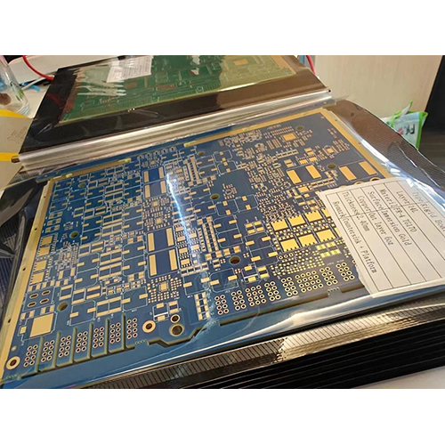
- Rigid, Multilayer, HDI
- 2-32 Layers (Standard: 4, 6, 8 Layers)
- 10% Controlled
- 0.075 mm (3 mil)
- High Frequency FR4 PCB HDI Assembly Multilayer PCB Circuit Board
- Yes
- Up to 10:1
- -40 C to +130 C
- SMT, THT, Mixed Assembly
- Customized, Standard HDI Stack-up Available
- Gold, Silver, Tin, OSP, HASL
- -20 C to +65 C
- 0.2 mm Min.
- Edge, Surface mount, Customizable
- Laser Microvia, Blind/Buried Vias
- Available
- 0.10 mm
- CNC, V-cut, Beveling, Scoring
Product Description
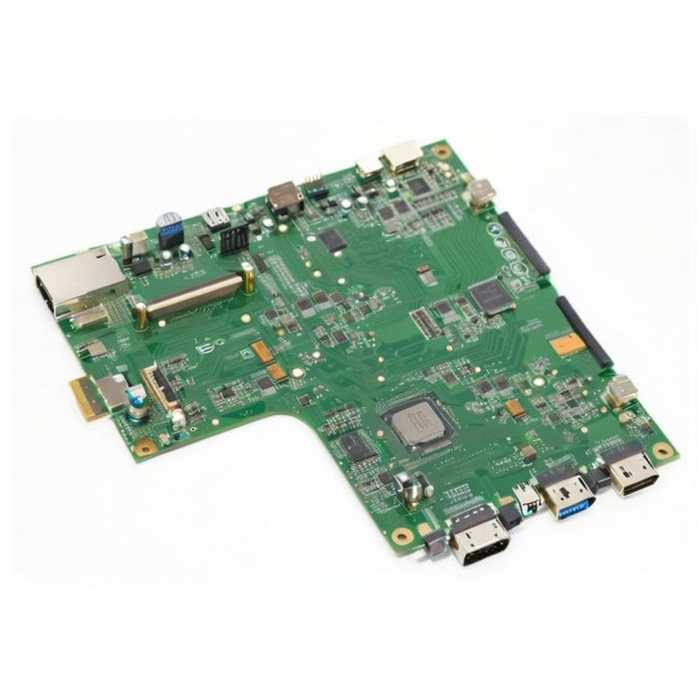
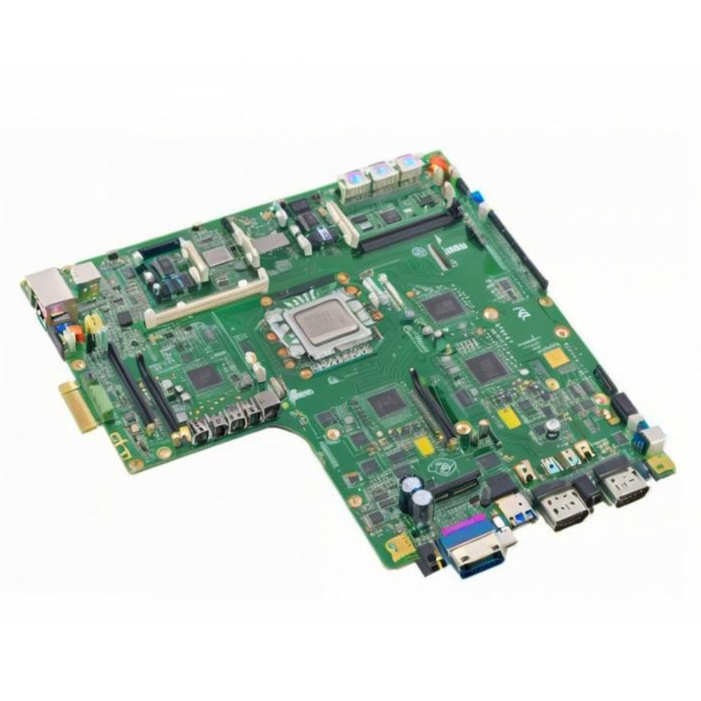
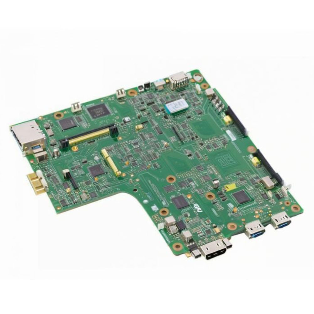
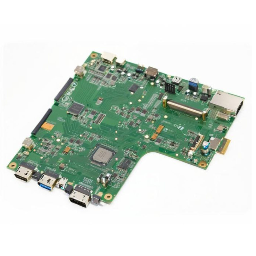
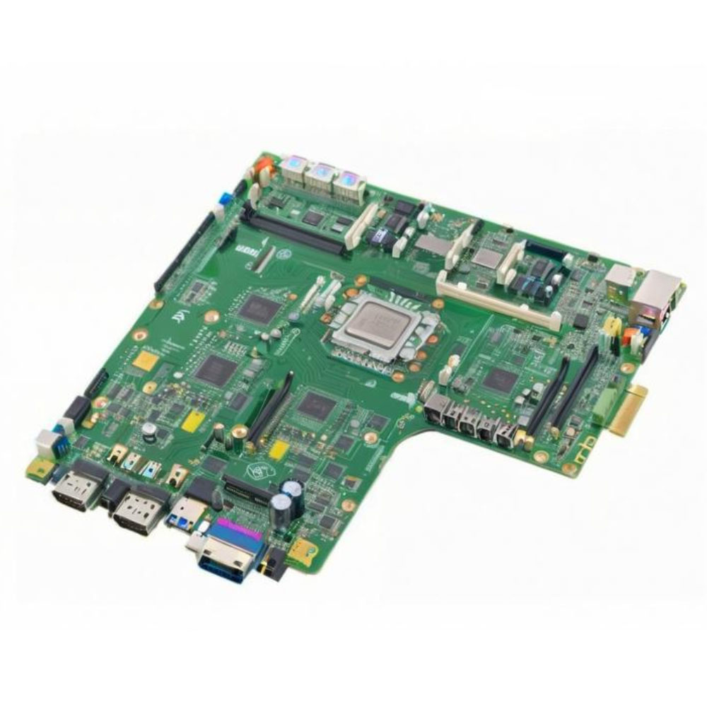
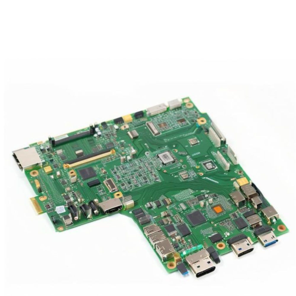
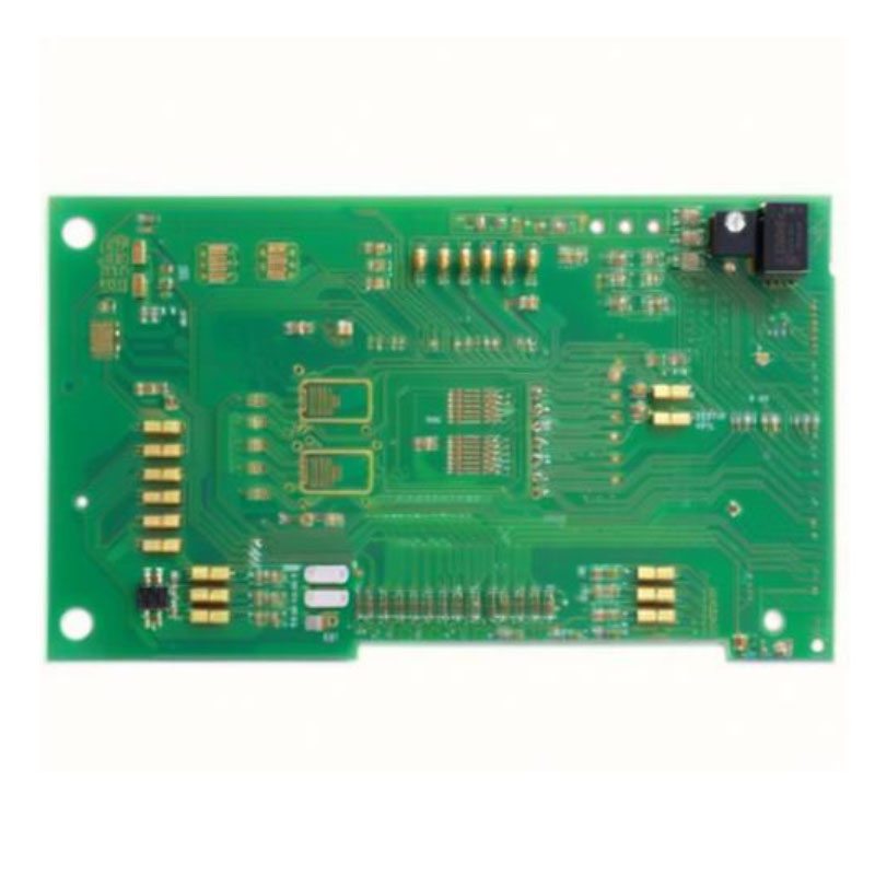
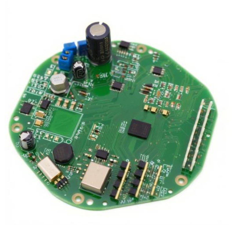
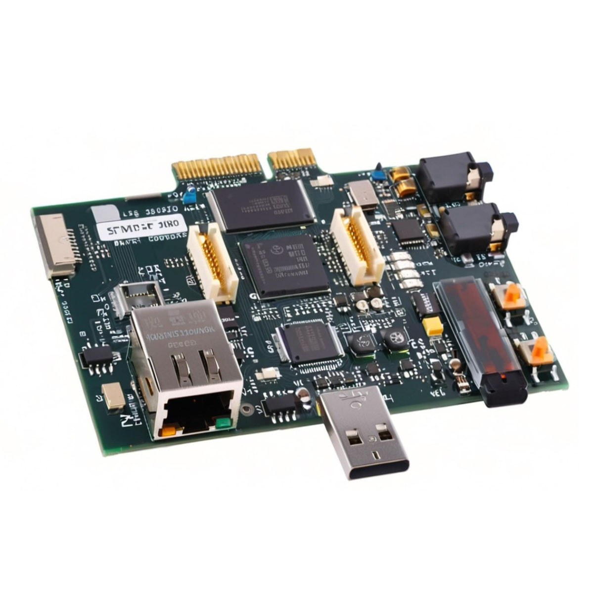
Spotlight your innovation with our Professional Custom High Frequency FR4 PCB HDI Assembly - a best-seller and a trending choice among industry leaders. Meticulously crafted for outstanding performance, this sensational multilayer circuit board supports stack-ups from 2 to 32 layers, offering famed HDI capabilities like laser microvia, blind and buried vias. Experience exceptional reliability, with pad plating options (gold, silver, tin, OSP, HASL) and comprehensive assembly services (SMT, THT, mixed). Customizable edge and surface-mount connectors, RoHS compliance, and superb finish tolerance place this PCB at the forefront of advanced manufacturing. Exported globally from India, it's your key to electrical excellence.
Applications & Directions for Use
This outstanding multilayer HDI PCB circuit board is ideal for use in high-frequency devices, telecommunications, medical instrumentation, industrial automation, consumer electronics, and automotive controls. Apply the board in both commercial and advanced research environments where signal integrity and component density matter. Integrate the famed PCB into your systems by following standard assembly procedures; its performance is optimized for use in mixed media, digital or analog signal applications, and diverse commercial-scale electronics projects.
Packaging, Samples, and Payment Information
Each PCB is delivered in robust, anti-static packaging to ensure safety and minimize transportation expenditure. We offer sample units to qualify your specific application requirements before bulk commitment. For commercial orders, our payment terms are flexible - designed to accommodate your unique business processes. Multiple panels can be shipped per carton, with tracking details provided, ensuring your consignment arrives securely and on schedule, allowing for confident investment and hassle-free ordering.
FAQ's of Professional Custom High Frequency Fr4 PCB Hdi Assembly Manufacturing Pcba Multilayer PCB Circuit Board:
Q: How can I customize the stack-up and layer count of the PCB for my project?
A: Simply provide your preferred stack-up and desired number of layers (2-32 layers supported) when placing your order. Our manufacturing team will tailor the PCB configuration to meet your precise requirements.Q: What testing and quality assurance processes are performed on these PCBs?
A: Each circuit board undergoes extensive 100% E-test, Automated Optical Inspection (AOI), and functional tests to guarantee reliability, conductivity, and conformity to your specifications.Q: Where can this multilayer PCB be used for optimal performance?
A: This PCB delivers outstanding results in high-frequency, data-heavy environments such as telecom infrastructure, automotive electronics, medical equipment, and industrial control systems, among many others.Q: What are the sample availability and lead times?
A: We provide sample boards for initial approval, with short lead times depending on complexity. Once samples are verified, bulk orders follow standard manufacturing timelines.Q: How does RoHS compliance benefit my commercial electronics projects?
A: RoHS compliance ensures your PCBs meet global environmental standards, reducing hazardous substances and supporting safer, sustainable product development.Tell us about your requirement

Price:
Quantity
Select Unit
- 50
- 100
- 200
- 250
- 500
- 1000+
Additional detail
Mobile number
Email

Other Products in 'Multilayer PCB' category
Contact Details
- No. 1506,15 Floor, SSG Tower, 561 ADien Bien Phu Str, Ward 25, Binh Thanh Dist, HCMC, Ho Chi Minh City - 717000, Thanh Pho Ho Chi Minh, Vietnam
- Ms. Yolanda Ke (Sales Account Manager)
- Mobile : +8613751081371
- Send Inquiry
NOVA TECHNOLOGY VIETNAMESE COMPANY LIMITED
|
 Call Me Free

NOVA TECHNOLOGY VIETNAMESE COMPANY LIMITED
All Rights Reserved.(Terms of Use)
Developed and Managed by Infocom Network Private Limited.
Developed and Managed by Infocom Network Private Limited.
