


PCBA circuit board design and drawing manufacturing factory assembly one-stop service supplier
Product Details:
- Min. Line Width 0.075mm
- Soldermask Green, Red, Blue, Black, Yellow, White
- Voltage Endurance 1500V
- Insulation Resistance >10^12
- Flame Resistance Level UL94-V0
- Silkscreen White, Black, Yellow
- Test Flying Probe, E-test, AOI, X-ray
- Click to view more
X
PCBA circuit board design and drawing manufacturing factory assembly one-stop service supplier Price And Quantity
- 1 Piece
- 1 Piece (prototype acceptable)
- Global (Europe, America, Asia, etc.)
- Prototype and Mass Production
- 3-15 Days Depending on Quantity
- Gerber, BOM, CAD, etc.
- RoHS, ISO9001, CE Certified
- OEM/ODM One-Stop Service
- ESD and Vacuum Packing
- Schematic & Layout Design Supported
- ICT, FCT, Burn-in, X-ray for BGA
- Full/Partial BOM Sourcing
PCBA circuit board design and drawing manufacturing factory assembly one-stop service supplier Product Specifications
- 0.075mm
- UL94-V0
- White, Black, Yellow
- Green/Blue/Black/Custom
- 1oz-3oz
- PCBA Circuit Board Design and Assembly
- >10^12
- 0.2mm-6.0mm
- 1500V
- Min 0.15mm
- Rigid, Flex, Rigid-Flex
- 10%
- Custom as per Design
- 0.075mm
- SMD, Through-hole, Mixed
- HASL, ENIG, OSP, Gold Plating (Custom)
- 1-24 Layers
- FR4, High TG, Rogers, Aluminum, CEM-1/CEM-3
- Optional/Customizable
- Flying Probe, E-test, AOI, X-ray
- Green, Red, Blue, Black, Yellow, White
- 1 Piece (prototype acceptable)
- Global (Europe, America, Asia, etc.)
- Prototype and Mass Production
- 3-15 Days Depending on Quantity
- Gerber, BOM, CAD, etc.
- RoHS, ISO9001, CE Certified
- OEM/ODM One-Stop Service
- ESD and Vacuum Packing
- Schematic & Layout Design Supported
- ICT, FCT, Burn-in, X-ray for BGA
- Full/Partial BOM Sourcing
Product Description
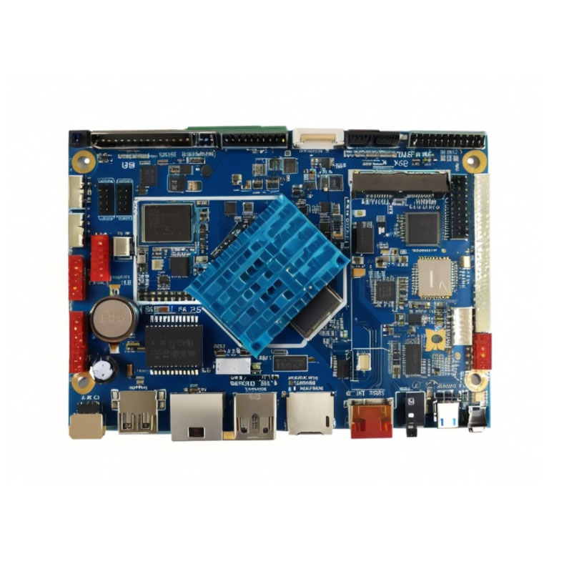
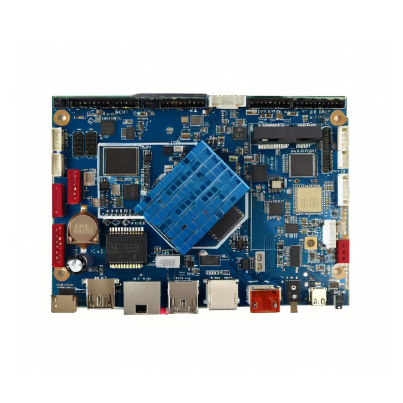
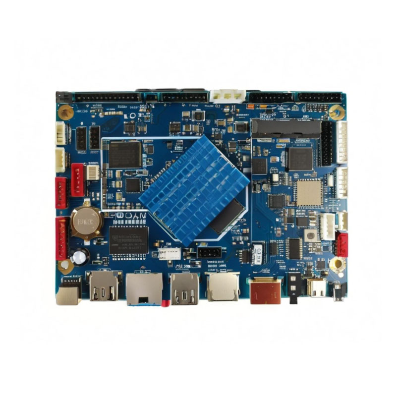
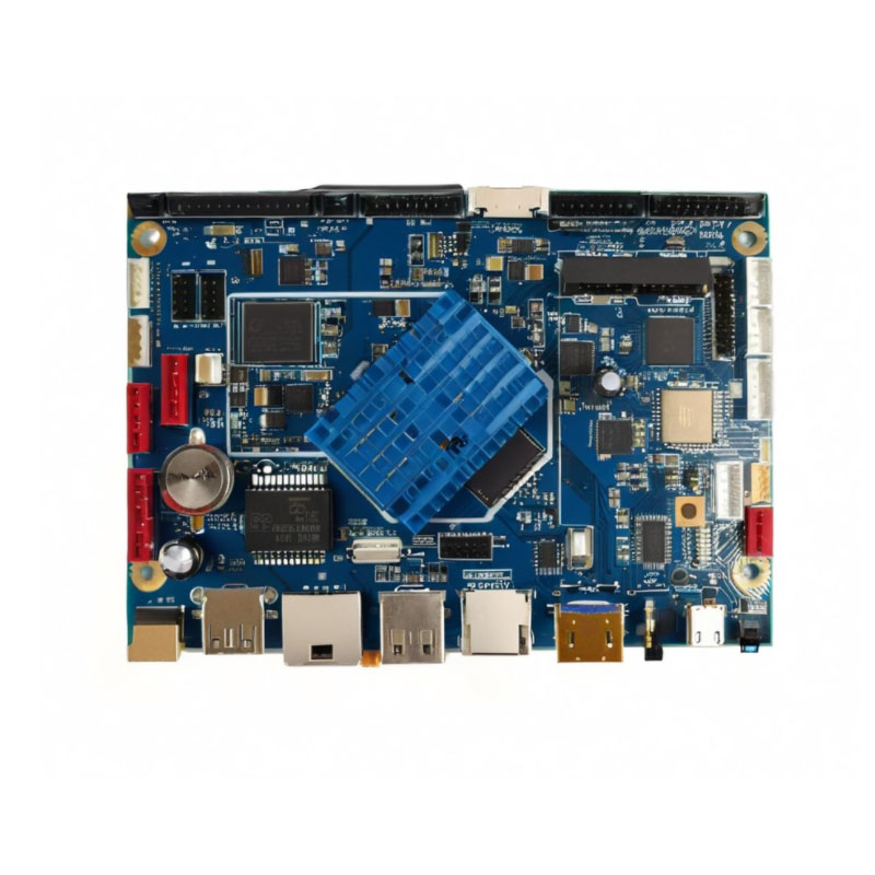
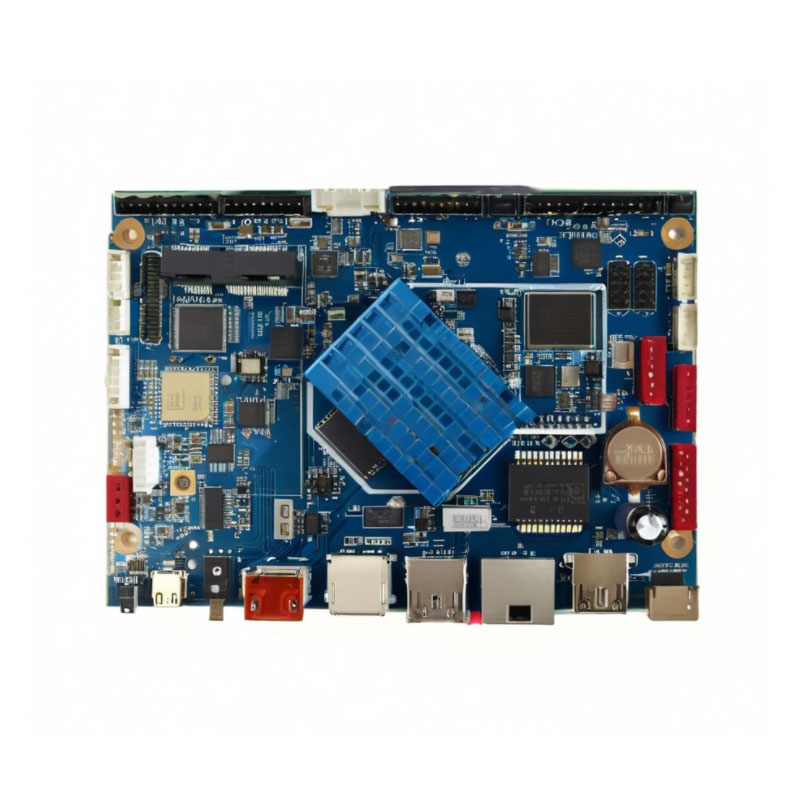
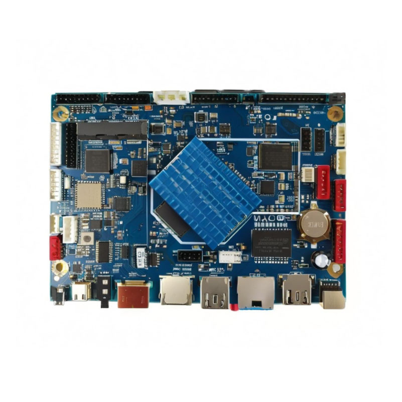
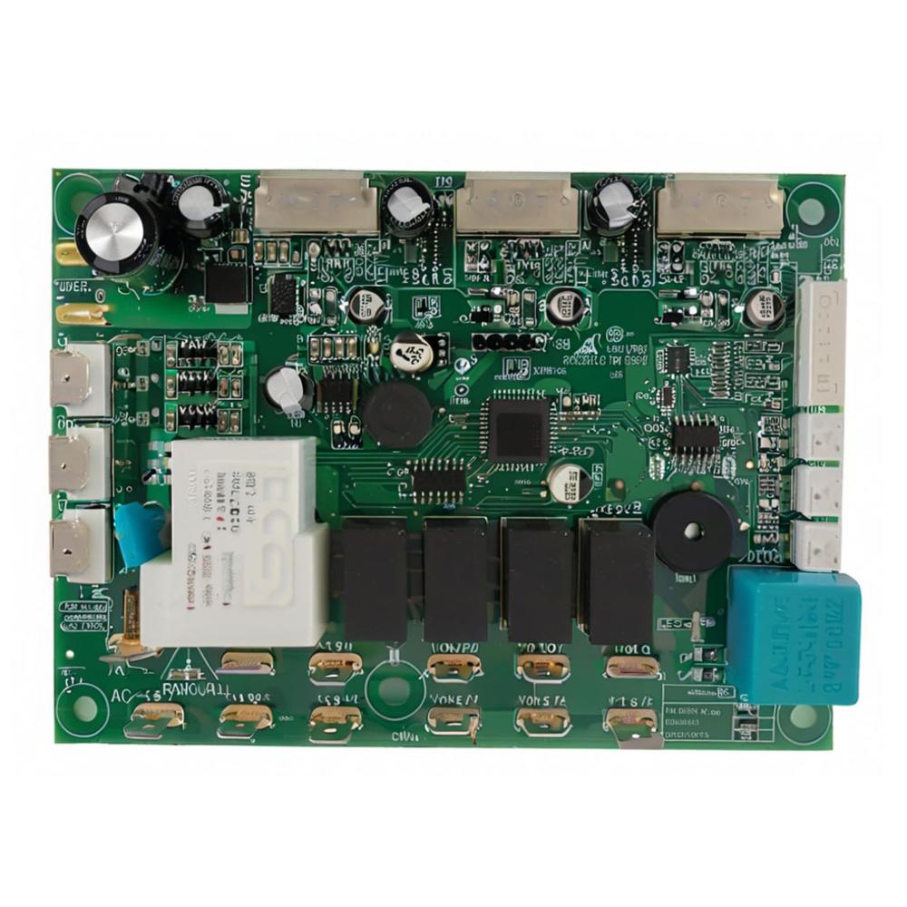
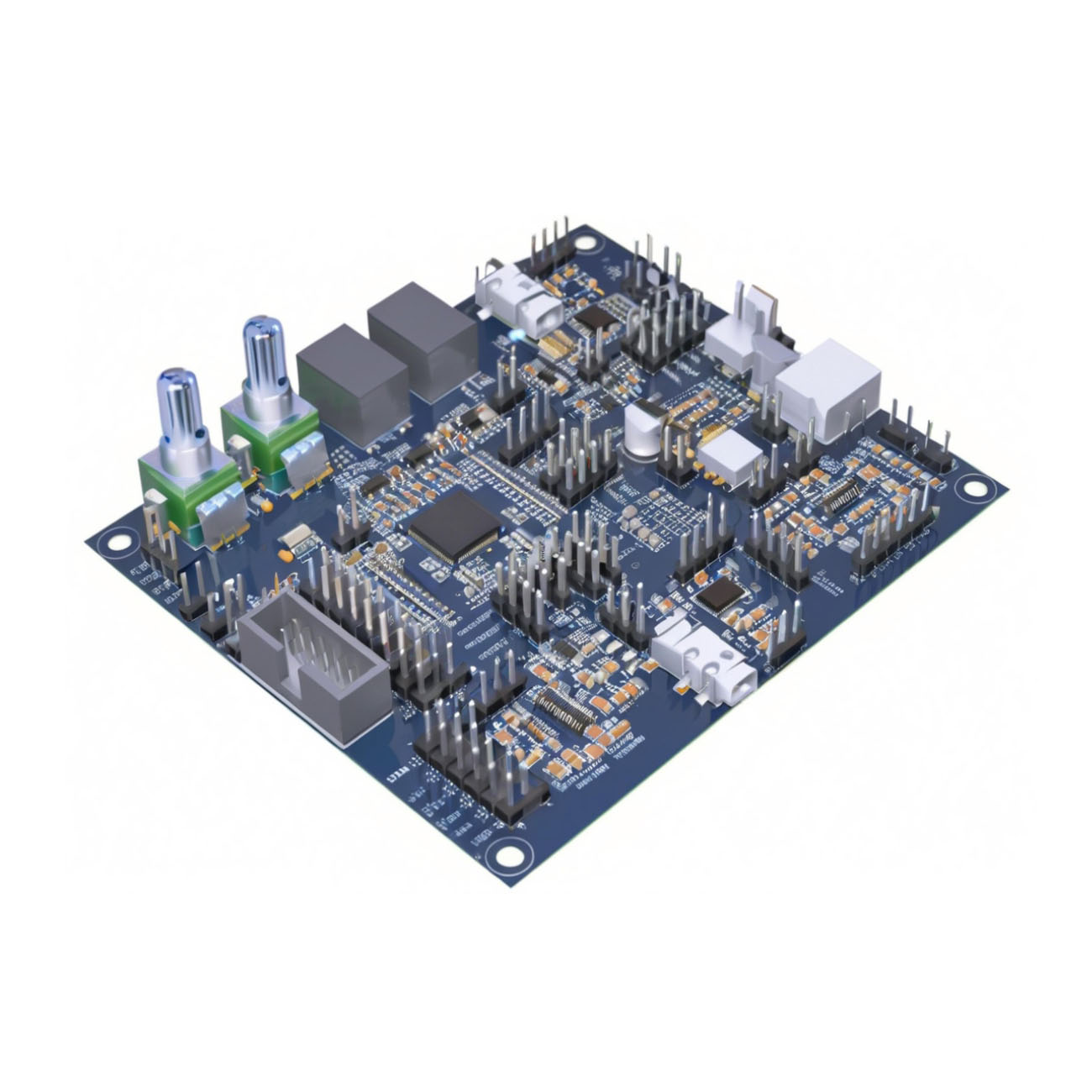
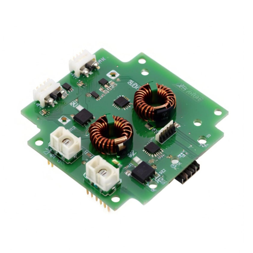
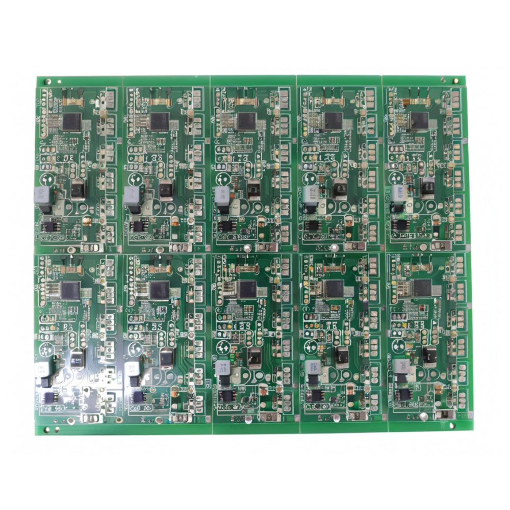
Experience majestic savings and uncompromising quality with our champion PCBA circuit board design and manufacturing factory. As a perfect one-stop service supplier, you can personalise and pick yours from prototype to mass production runs. Supported by advanced schematic and layout design services, we excel in full or partial BOM sourcing and rigorous testing, including ICT, FCT, and X-ray for BGAs. Our compliant, ISO9001, CE-certified facilities support a variety of colors, surface finishes, and custom panel sizes-delivering the ultimate OEM/ODM solutions worldwide, with an MOQ of just one piece.
Versatile Application Areas & Usage
Our one-stop PCBA circuit board design and assembly services are an ideal choice for diverse sectors including telecommunications, automotive, medical devices, and consumer electronics. With custom sensor switch options and compatibility for both SMD and through-hole components, you can perfectly tailor your boards. Simply submit your files in Gerber, BOM, or CAD formats, and we'll turn your designs into reliable, production-ready PCBA assemblies for your specific usage needs.
Packaging, Shipment & Domestic Market
We prioritize secure packaging with ESD and vacuum packing to guarantee your PCBA's integrity. Our main domestic market is India, with global export capabilities. Flexible payment terms ensure customer satisfaction, and sample availability lets you verify quality before final orders. For asking price or shipment details, reach out and experience seamless support from your first inquiry through to prompt delivery-every step packaged to perfection.
FAQ's of PCBA circuit board design and drawing manufacturing factory assembly one-stop service supplier:
Q: How does your PCBA design and manufacturing process work?
A: Our process begins with your design files (Gerber, BOM, CAD, etc.), followed by schematic and layout design support, component sourcing as required, assembly (from prototype to mass production), and comprehensive testing (ICT, FCT, AOI, X-ray). Every step is tailored to meet your specific requirements.Q: What testing methods do you use to ensure product quality?
A: We employ multiple testing procedures, including ICT, FCT, AOI, flying probe, burn-in, and X-ray (especially for BGAs), ensuring that every PCBA meets strict standards before shipment.Q: Where can your PCBA services be exported to?
A: We export globally, supplying PCBA solutions to markets in Europe, America, Asia, and beyond, in addition to serving the Indian domestic market.Q: When can I expect my order to be delivered?
A: Lead times vary by order quantity, typically ranging from 3 to 15 days. After finalizing your design and order, we provide you with a more precise delivery estimate.Q: What are the benefits of choosing your one-stop PCBA service?
A: Opting for our one-stop solution means savings on time and cost, as we handle everything from design and sourcing to assembly and testing-ensuring seamless and reliable delivery tailored to your project needs.Q: How do I request a sample or get a quotation?
A: Simply contact us with your requirements and design files. We provide samples for evaluation, and our team will respond promptly with a customized asking price and shipment options.Tell us about your requirement

Price:
Quantity
Select Unit
- 50
- 100
- 200
- 250
- 500
- 1000+
Additional detail
Mobile number
Email

Other Products in 'PCBA Customized' category
Contact Details
- No. 1506,15 Floor, SSG Tower, 561 ADien Bien Phu Str, Ward 25, Binh Thanh Dist, HCMC, Ho Chi Minh City - 717000, Thanh Pho Ho Chi Minh, Vietnam
- Ms. Yolanda Ke (Sales Account Manager)
- Mobile : +8613751081371
- Send Inquiry
NOVA TECHNOLOGY VIETNAMESE COMPANY LIMITED
|
 Call Me Free

NOVA TECHNOLOGY VIETNAMESE COMPANY LIMITED
All Rights Reserved.(Terms of Use)
Developed and Managed by Infocom Network Private Limited.
Developed and Managed by Infocom Network Private Limited.
