


PCB maker Full experience in pcba pcb assembly SMD, PTH and mixture both with wave soldering Supplier
Product Details:
- Hole Size Min. 0.2mm, custom as required
- Soldermask Green, Red, Blue, Black, Yellow, White; custom colors possible
- Min. Line Spacing 0.075mm (3mil)
- Impedance Controlled impedance 10%
- Voltage Endurance AC 3000V/Minute
- Silkscreen
- Board Type Rigid, Flexible, Rigid-Flex
- Click to view more
X
PCB maker Full experience in pcba pcb assembly SMD, PTH and mixture both with wave soldering Supplier Price And Quantity
- INR
- 1
- Yes, laser-cut stainless steel stencil
- Edge Connectors, Custom Connectors
- Prototype, Low to High Volume Production
- Yes, BOM procurement to final testing
- Both Through-Hole and SMT
- 0.3mm
- Wave Soldering and Reflow Soldering supported
- Sample 3-7 days, Mass production 7-15 days
- 0.05mm (50m)
- Any, including complex contours
- Up to 50,000 CPH
- Supported
PCB maker Full experience in pcba pcb assembly SMD, PTH and mixture both with wave soldering Supplier Product Specifications
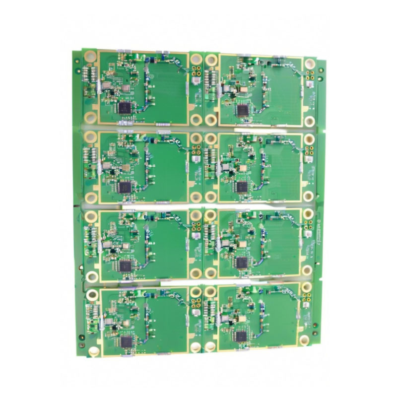
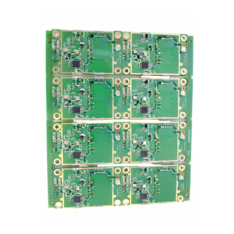
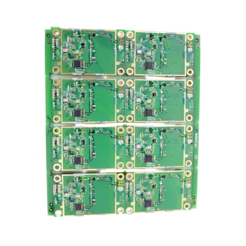
- Comprehensive SMD & PTH placement, passive and active components
- UL 94V-0
- AC 3000V/Minute
- Controlled impedance 10%
- On request, customizable
- Green, Red, Blue, Black, Yellow, White; custom colors possible
- 0.075mm (3mil)
- Min. 0.2mm, custom as required
- 1-24 layers standard
- >10^12 (Ohms)
- PCB Assembly (SMT, PTH, Mixed)
- 0.075mm (3mil)
- Green, Blue, Red, Yellow, Black, White
- 1.6mm typical, customizable from 0.5mm-3.0mm
- Rigid, Flexible, Rigid-Flex
- HASL, Lead-Free HASL, ENIG, OSP, Immersion Silver/Tin, Gold Finger
- FR4, CEM1, CEM3, High TG, Aluminum, Rogers
- Up to 600mm x 1200mm
- 1oz (35um) standard, custom options from 0.5-6oz
- AOI, X-ray, Flying Probe, ICT, Functional Test
- Yes, laser-cut stainless steel stencil
- Edge Connectors, Custom Connectors
- Prototype, Low to High Volume Production
- Yes, BOM procurement to final testing
- Both Through-Hole and SMT
- 0.3mm
- Wave Soldering and Reflow Soldering supported
- Sample 3-7 days, Mass production 7-15 days
- 0.05mm (50m)
- Any, including complex contours
- Up to 50,000 CPH
- Supported
Product Description
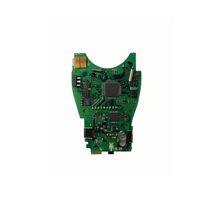
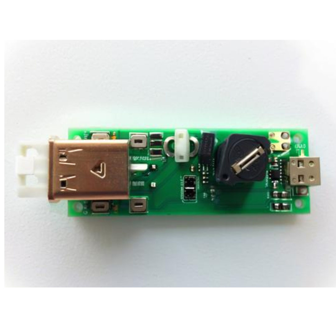
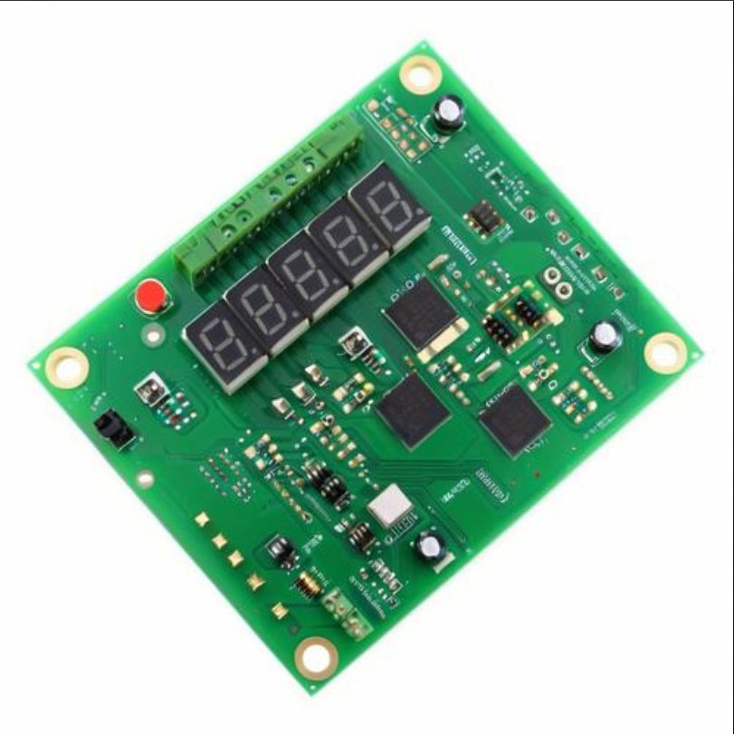
Experience the fresh paragon of PCB assembly with India's gilt-edged supplier, ending soon for select offers! Buy online to avail grandiose capabilities-Full PCB maker with PCBA, SMD, PTH, and hybrid assembly with wave/reflow soldering. Achieve stellar component placement accuracy down to 0.05mm, handle BGA ball sizes to 0.3mm, and enjoy turnkey services from BOM to quality-tested final product. Prototype through high-volume production supported. Multiple customizations: color, board shape, thickness, layers, and connectors. Delivering premium quality with rapid lead time-samples in 3-7 days, mass runs in 7-15. Upgrade to a benchmark in PCB excellence now!
End-to-End PCB Services: Applications, Features, and Surface Reach
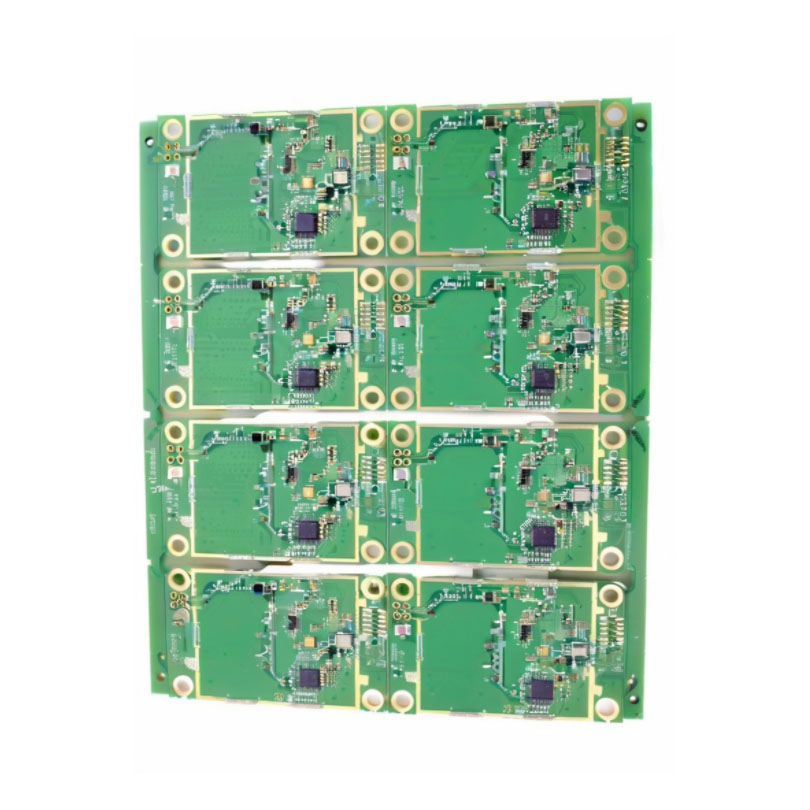
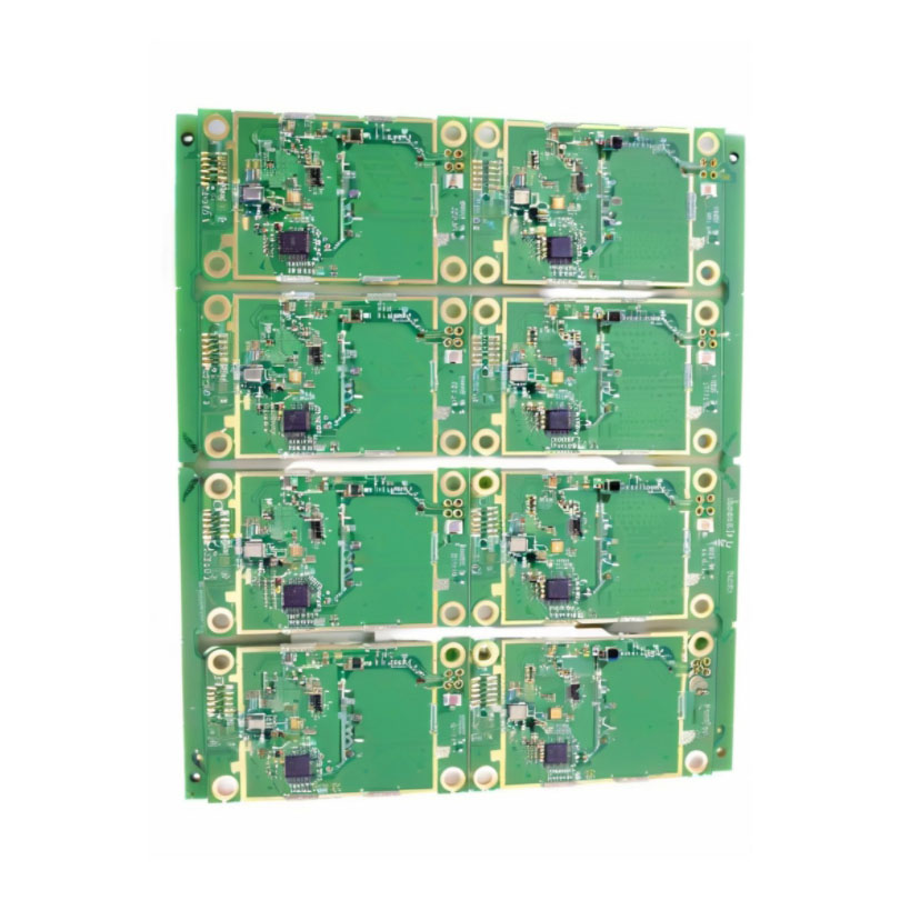
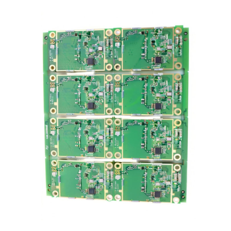
With comprehensive expertise, our PCB maker excels in pcba, SMD, PTH, and hybrid wave soldering for varied industries like automotive, telecom, medical, and industrial automation. Special features include castellated holes, controlled-impedance routing, and support for custom connectors with all board types-rigid, flex, and rigid-flex. PCBs are suitable for any application surface-greenfield innovations, replacement modules, or premium defense systems. Each board undergoes robust AOI, X-ray, and functional testing for gilt-edged reliability.
Premium Domestic Market Coverage: Packing, Dispatch, and Timely Delivery
Our packing & dispatch processes are engineered for premium protection and prompt logistics, ensuring deliveries across all major domestic markets in India. With FOB port access at major Indian seaports, customers enjoy hassle-free international and local shipments. Typical delivery time for samples is 3-7 days, and bulk production is dispatched within 7-15 days. Our reliable systems keep every order secure, allowing seamless scale-up from prototype to mass production efficiently.
End-to-End PCB Services: Applications, Features, and Surface Reach
With comprehensive expertise, our PCB maker excels in pcba, SMD, PTH, and hybrid wave soldering for varied industries like automotive, telecom, medical, and industrial automation. Special features include castellated holes, controlled-impedance routing, and support for custom connectors with all board types-rigid, flex, and rigid-flex. PCBs are suitable for any application surface-greenfield innovations, replacement modules, or premium defense systems. Each board undergoes robust AOI, X-ray, and functional testing for gilt-edged reliability.
Premium Domestic Market Coverage: Packing, Dispatch, and Timely Delivery
Our packing & dispatch processes are engineered for premium protection and prompt logistics, ensuring deliveries across all major domestic markets in India. With FOB port access at major Indian seaports, customers enjoy hassle-free international and local shipments. Typical delivery time for samples is 3-7 days, and bulk production is dispatched within 7-15 days. Our reliable systems keep every order secure, allowing seamless scale-up from prototype to mass production efficiently.
FAQ's of PCB maker Full experience in pcba pcb assembly SMD, PTH and mixture both with wave soldering Supplier:
Q: How accurate is the component placement in your PCB assembly service?
A: Our assembly boasts a placement accuracy of 0.05mm (50 microns), ensuring precise production for both fine-pitch and complex components.Q: What special features distinguish your PCB manufacturing process?
A: We support features such as wave and reflow soldering, controlled impedance, half-hole/castellated holes, and comprehensive connector support including edge and custom variants.Q: When can customers expect delivery after an online purchase?
A: Samples are typically shipped within 3-7 days, while mass production orders are dispatched within 7-15 days following order confirmation and BOM approval.Q: Where are your PCB assembly and manufacturing services available?
A: Our PCBA manufacturing is based in India, with both export and all-India domestic market service, and shipment options through major FOB ports.Q: What is the process for ordering and receiving a turnkey PCB assembly?
A: Customers can buy online, provide their BOM, and we handle procurement, assembly, testing, and shipping to deliver a complete, ready-to-use product.Q: How can clients benefit from your comprehensive PCB services?
A: Clients enjoy a one-stop solution from prototype to high-volume runs, customizable boards, rapid lead times, robust testing, and expert support throughout.Q: What types of testing are performed on finished PCBs?
A: Each board undergoes thorough AOI, X-ray inspection, Flying Probe, ICT, and functional tests to ensure high quality and reliability.Tell us about your requirement

Price:
Quantity
Select Unit
- 50
- 100
- 200
- 250
- 500
- 1000+
Additional detail
Mobile number
Email

Other Products in 'PCBA Customized' category
Contact Details
- No. 1506,15 Floor, SSG Tower, 561 ADien Bien Phu Str, Ward 25, Binh Thanh Dist, HCMC, Ho Chi Minh City - 717000, Thanh Pho Ho Chi Minh, Vietnam
- Ms. Yolanda Ke (Sales Account Manager)
- Mobile : +8613751081371
- Send Inquiry
NOVA TECHNOLOGY VIETNAMESE COMPANY LIMITED
|
 Call Me Free

NOVA TECHNOLOGY VIETNAMESE COMPANY LIMITED
All Rights Reserved.(Terms of Use)
Developed and Managed by Infocom Network Private Limited.
Developed and Managed by Infocom Network Private Limited.
