


One Stop Customized development pcb&pcba and Design of Embedded Control Board Scheme for PCB Circuit Board Electronics Supplier
Product Details:
- Test E-test, AOI, Function Test as required
- Voltage Endurance 1.5kV - 3.0kV
- Min. Line Width 0.075mm
- Insulation Resistance >20M
- Min. Line Spacing 0.075mm
- Flame Resistance Level UL94-V0
- Silkscreen White, Black, Yellow (customizable)
- Click to view more
X
One Stop Customized development pcb&pcba and Design of Embedded Control Board Scheme for PCB Circuit Board Electronics Supplier Price And Quantity
- 1
- INR
- Yes, OEM/ODM
- Vacuum & Anti-static Packing
- 3-25 days depending on order and complexity
- -40C to +85C, material dependent
- Single or double side plating and assembly
- Available, includes schematic and firmware design
- SMT, Through Hole, Mixed
- Dry, Room Temperature
- Supported
- 0.05mm
One Stop Customized development pcb&pcba and Design of Embedded Control Board Scheme for PCB Circuit Board Electronics Supplier Product Specifications
- 0.075mm
- >20M
- Green, Blue, Black, Red, White (customizable)
- Optional, as per design requirements
- Rigid, Flexible, Rigid-Flex
- One Stop Customized Development PCB & PCBA, Embedded Control Board Scheme
- 1-24 layers
- up to 600mm x 1200mm
- 0.075mm
- SMT, DIP, Connectors, MCU, ICs, Sensors, Relays
- Min. 0.2mm
- 0.4mm - 3.2mm
- HASL, ENIG, OSP, Immersion Tin/Silver, Gold plating
- UL94-V0
- E-test, AOI, Function Test as required
- 1.5kV - 3.0kV
- White, Black, Yellow (customizable)
- Green, Blue, Black, Red, White (customizable)
- 1 oz - 3 oz
- FR4, CEM1, CEM3, High TG, Aluminum, Rogers
- 10% controlled impedance
- Yes, OEM/ODM
- Vacuum & Anti-static Packing
- 3-25 days depending on order and complexity
- -40C to +85C, material dependent
- Single or double side plating and assembly
- Available, includes schematic and firmware design
- SMT, Through Hole, Mixed
- Dry, Room Temperature
- Supported
- 0.05mm
Product Description
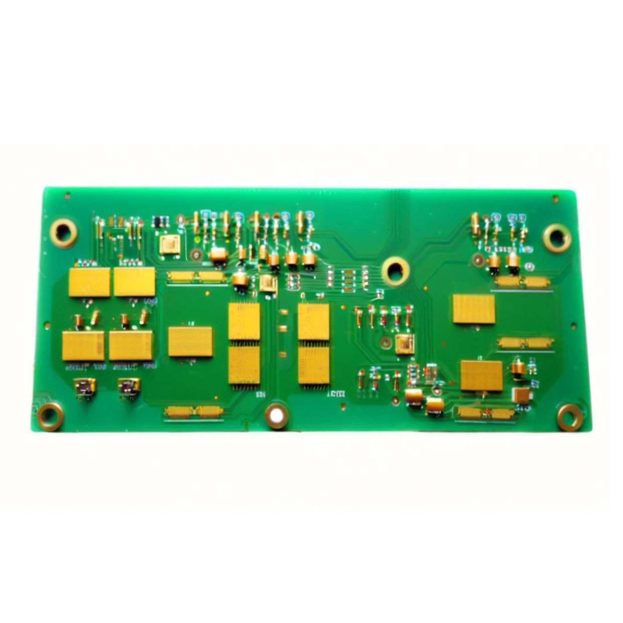
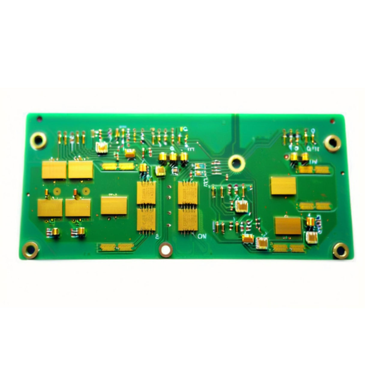
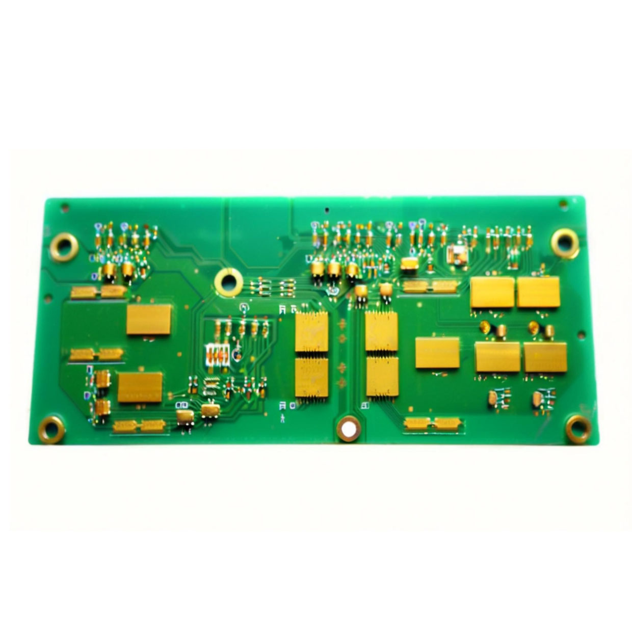
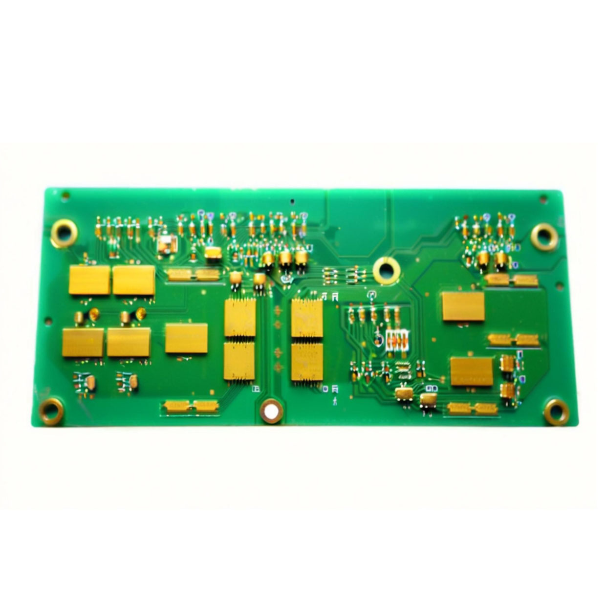
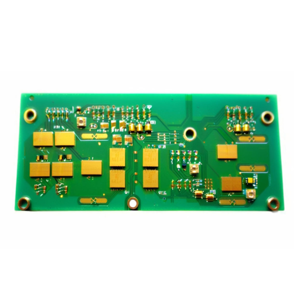
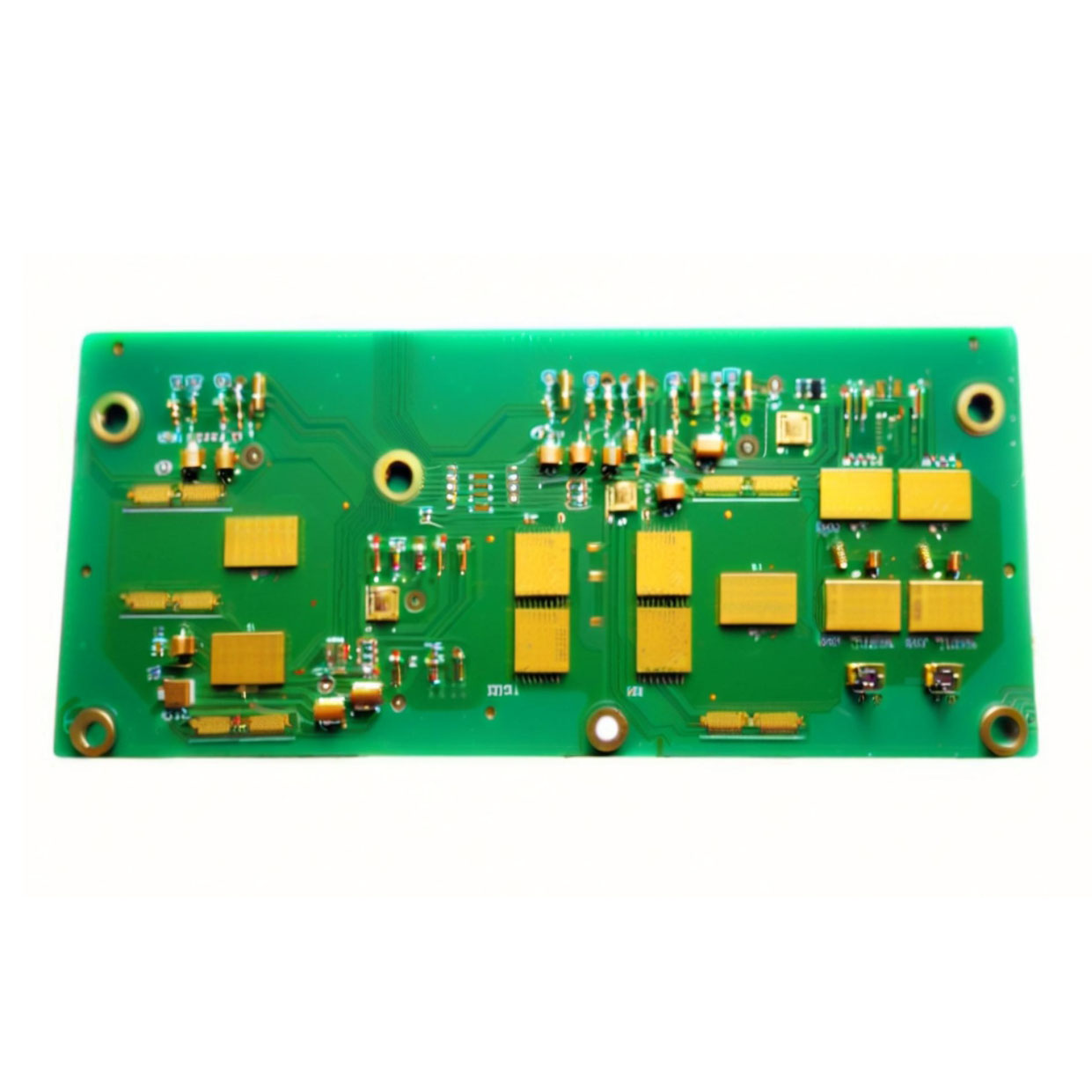
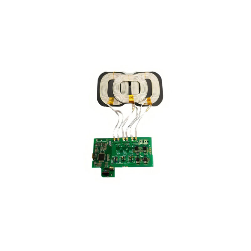
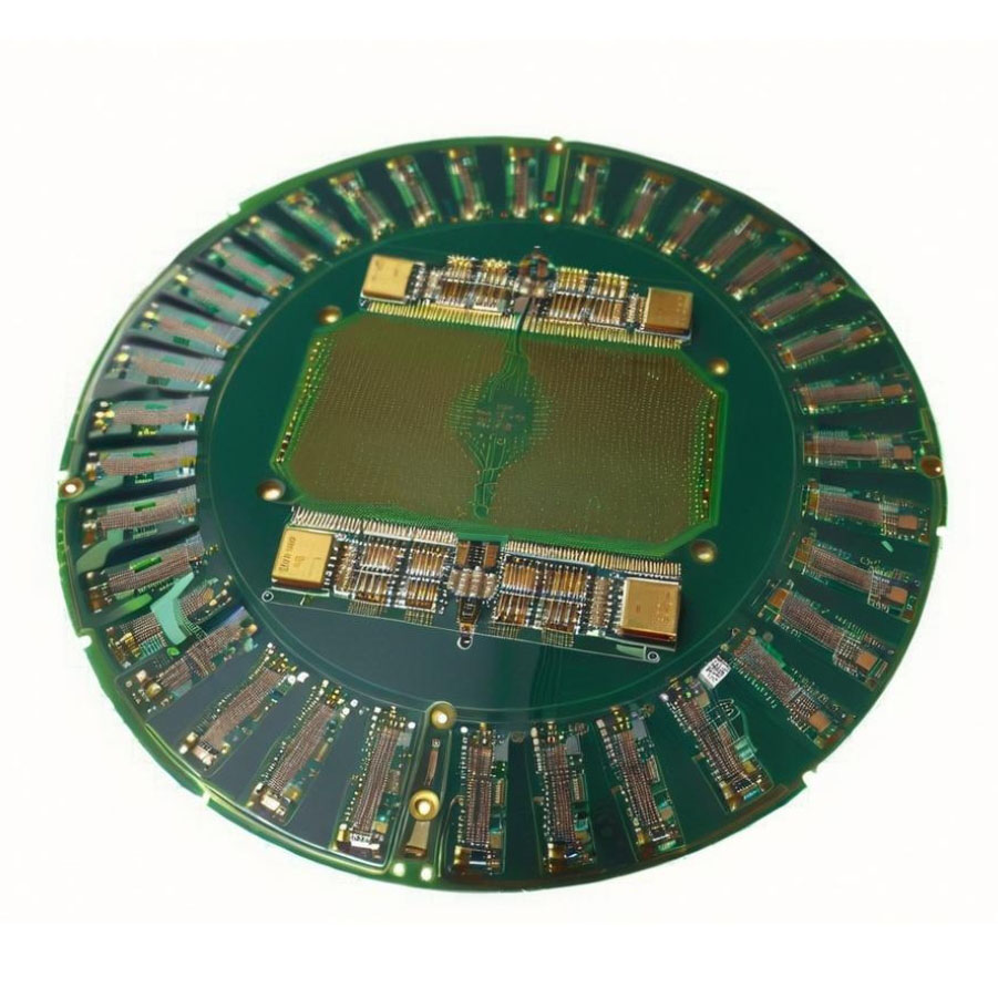
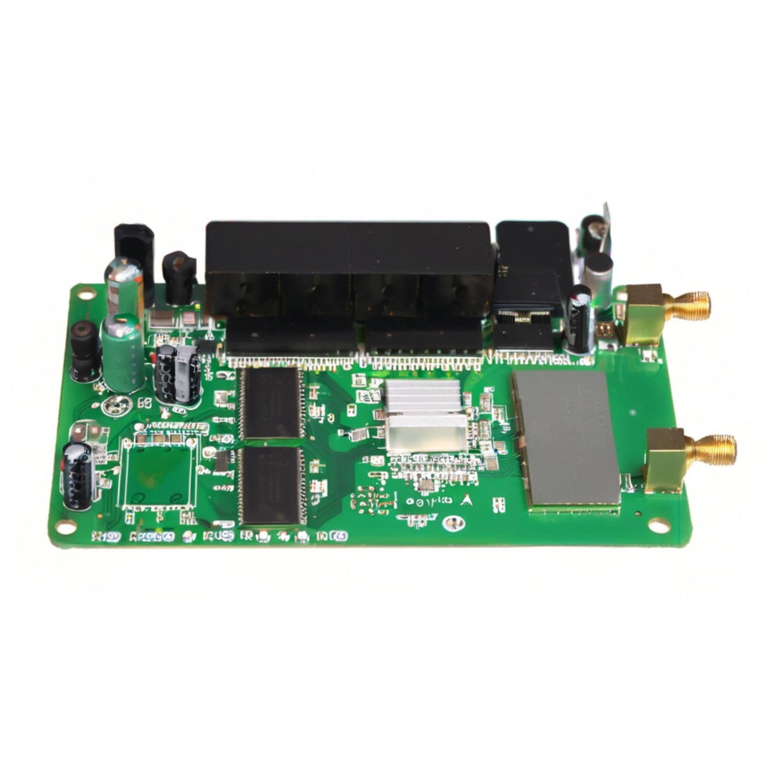
Distinguished by exceptional component assembly accuracy of 0.05mm, our one-stop customized development for PCB & PCBA brings magnificent flexibility and imposing capabilities to your electronics project. Personalise every detail-choose from various PCB types, finishes, colors, and silkscreen options-ensuring a tailored fit for rare or advanced embedded control board schemes. Our end-to-end service encompasses schematic, firmware design, and precise assembly (SMT, through-hole, or mixed). Benefit from rapid lead times (3-25 days), robust production material selection, and secure packaging. Suitable for demanding environments (-40C to +85C), our solutions guarantee reliability and innovation.
Versatile Applications Across Key Industries
Our new, state-of-the-art PCB & PCBA development is uniquely suitable for distinguished usage in industrial automation, automotive systems, consumer electronics, medical devices, energy, and IoT solutions. These advanced embedded control boards excel in handling signal processing, power management, and sensor integration across multiple application media. From laboratories to field installations, their imposing construction meets the requirements of both high- and low-voltage environments, proving indispensable in R&D, production, and mission-critical area of application.
Swift Proposal, Timely Dispatch, and Expansive Delivery Reach
With competitive proposal amounts tailored to your specific needs, our team ensures rate-efficient and quick dispatch of orders across India's leading markets. Delivery time scales dynamically, from 3 to 25 days, based on order complexity and quantity. Our scalable supply ability consistently supports bulk and bespoke requirements, facilitating prompt delivery to your doorstep-ensuring both rapid prototyping and large-scale production for OEM/ODM clients.
FAQ's of One Stop Customized development pcb&pcba and Design of Embedded Control Board Scheme for PCB Circuit Board Electronics Supplier:
Q: How can I customise the PCB design to fit my specific requirements?
A: You can personalise every aspect of your PCB, including board type, color, thickness, assembly method (SMT, through-hole, or mixed), and silkscreen. Our engineering team will support you from schematic layout to firmware design, ensuring a tailored solution that precisely matches your application.Q: What is the delivery lead time for prototype and large-volume PCB/PCBA orders?
A: Depending on the proposal amount and complexity, our dispatch time ranges from 3 days for quick prototypes to 25 days for more intricate or bulk orders. We prioritise both prompt service and production quality across all order sizes.Q: Where are your PCB & PCBA services available and delivered?
A: We supply our products across all major domestic markets throughout India. Our logistics framework is optimised for reliable delivery, whether for rapid samples or large production shipments.Q: What process is followed from design proposal to final assembly and testing?
A: The process starts with your requirements analysis and proposal, followed by schematic and firmware design. We proceed with prototyping, assembly (single or double side), and comprehensive testing (E-test, AOI, functional test as needed) before secure packaging and delivery.Q: What are the main benefits of using your one-stop PCB development and assembly services?
A: Clients benefit from streamlined project management, precision assembly with 0.05mm accuracy, flexible customization (including OEM/ODM support), and advanced quality control to ensure robust performance-even in demanding environments.Q: What types of electronic components and board materials do you support?
A: Our services cover SMT, DIP, connectors, MCUs, ICs, sensors, and relays. We work with a wide range of materials including FR4, CEM1, CEM3, High TG, Aluminum, and Rogers, catering to diverse industrial needs and specific applications.Tell us about your requirement

Price:
Quantity
Select Unit
- 50
- 100
- 200
- 250
- 500
- 1000+
Additional detail
Mobile number
Email

Other Products in 'PCBA Customized' category
Contact Details
- No. 1506,15 Floor, SSG Tower, 561 ADien Bien Phu Str, Ward 25, Binh Thanh Dist, HCMC, Ho Chi Minh City - 717000, Thanh Pho Ho Chi Minh, Vietnam
- Ms. Yolanda Ke (Sales Account Manager)
- Mobile : +8613751081371
- Send Inquiry
NOVA TECHNOLOGY VIETNAMESE COMPANY LIMITED
|
 Call Me Free

NOVA TECHNOLOGY VIETNAMESE COMPANY LIMITED
All Rights Reserved.(Terms of Use)
Developed and Managed by Infocom Network Private Limited.
Developed and Managed by Infocom Network Private Limited.
