Product Description
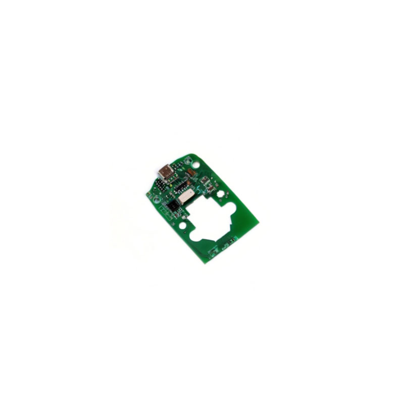
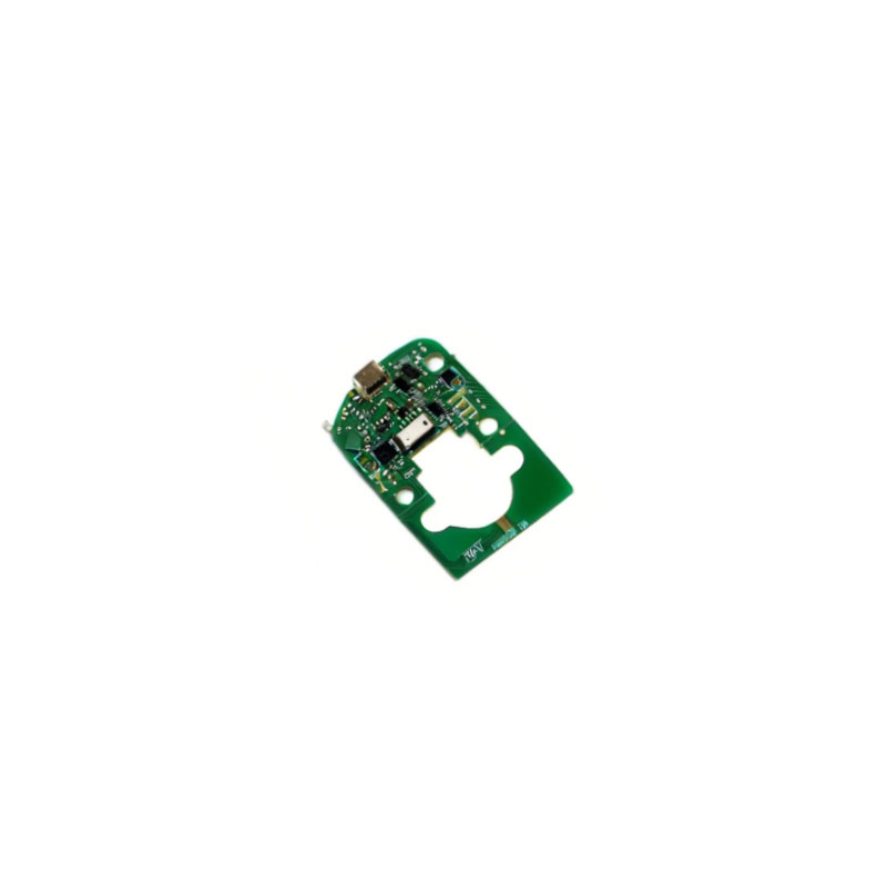
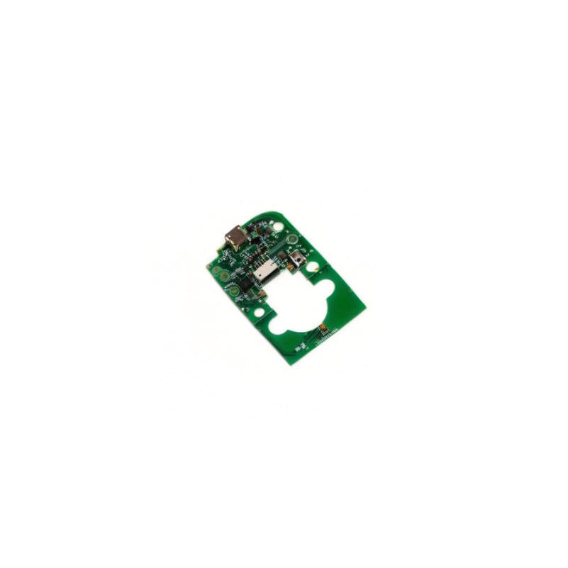
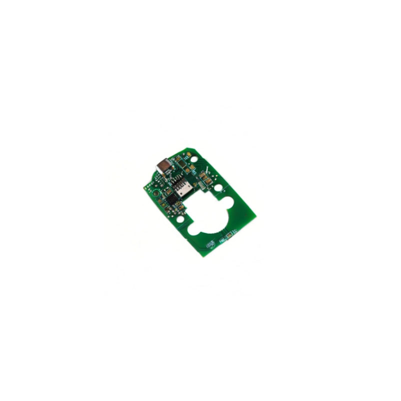
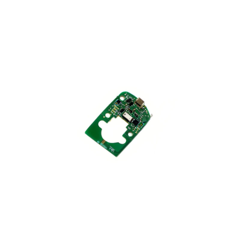
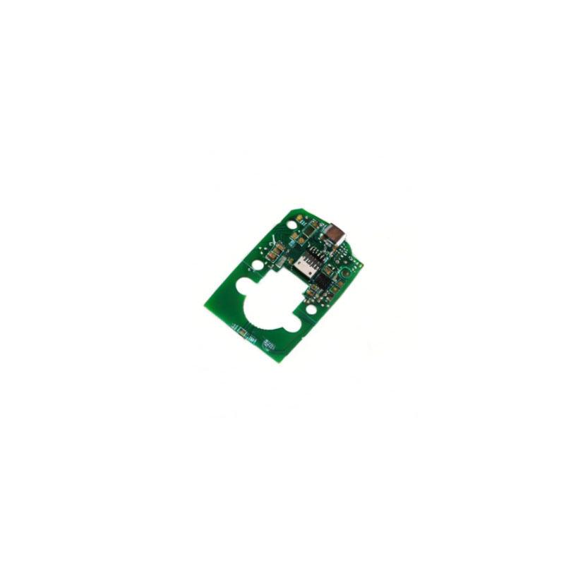
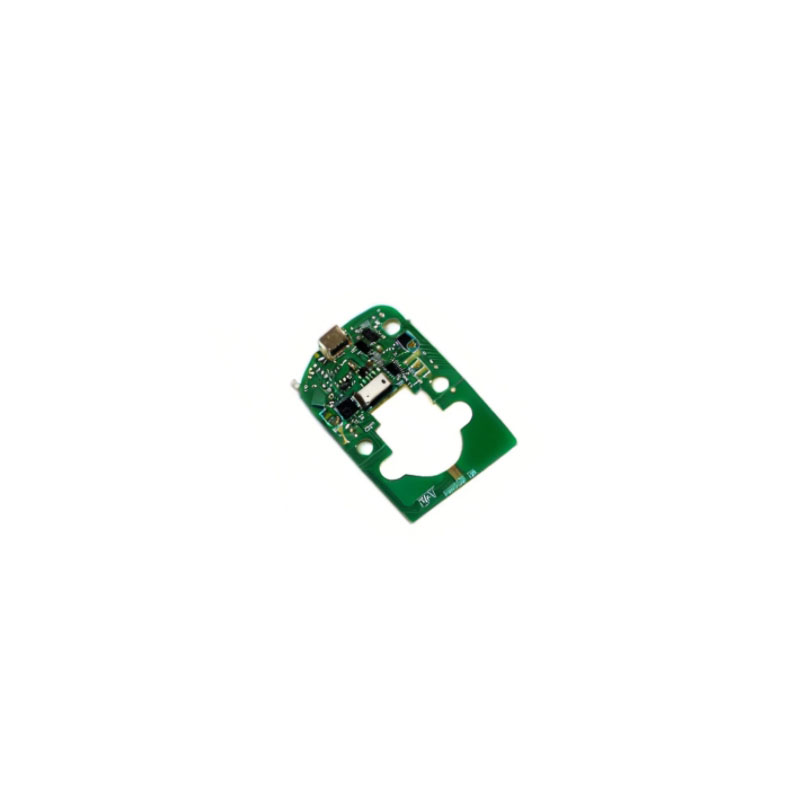
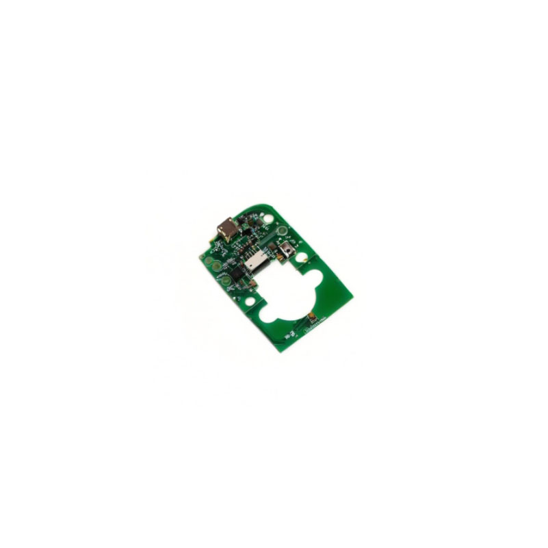
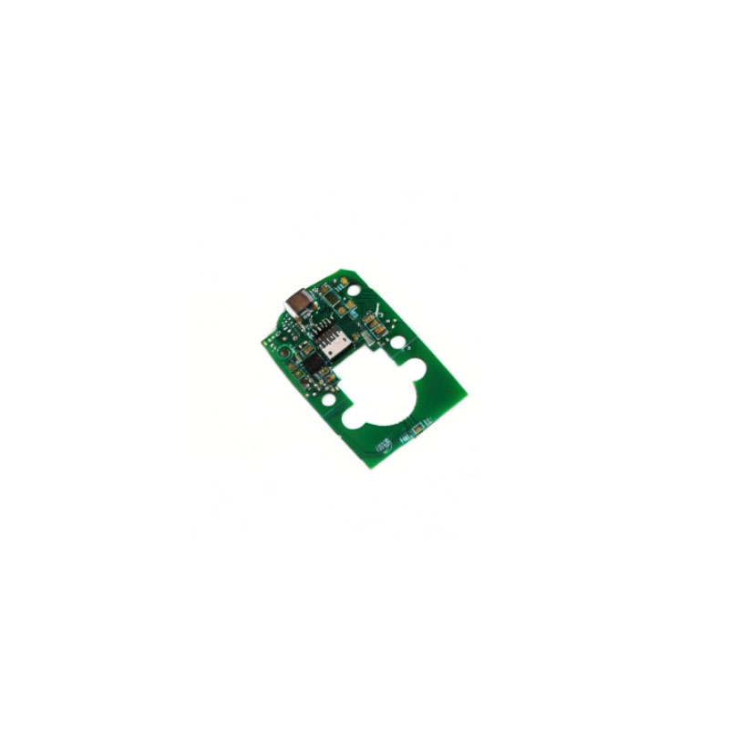
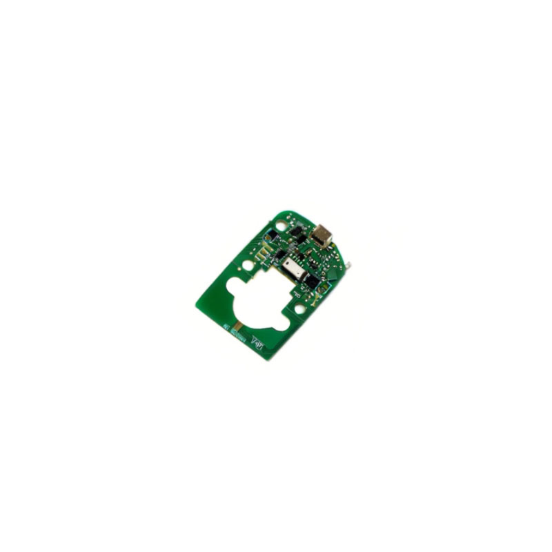
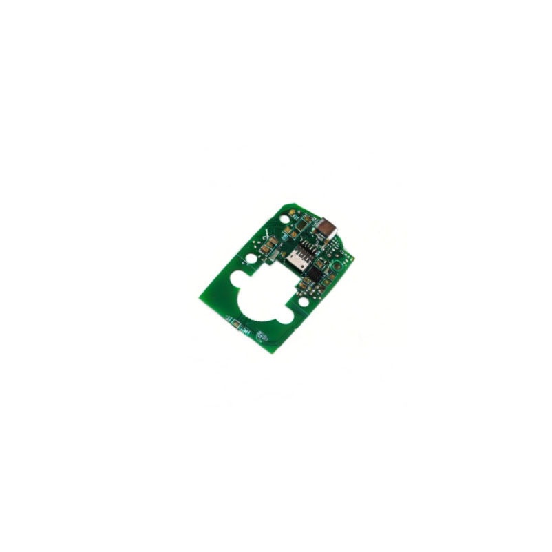
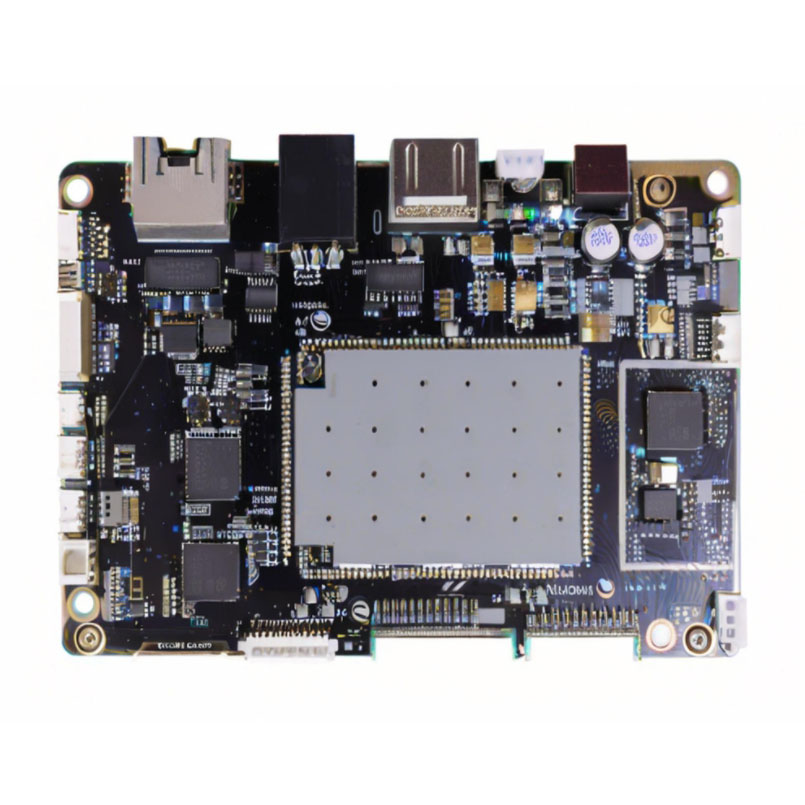
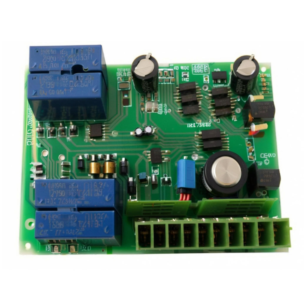
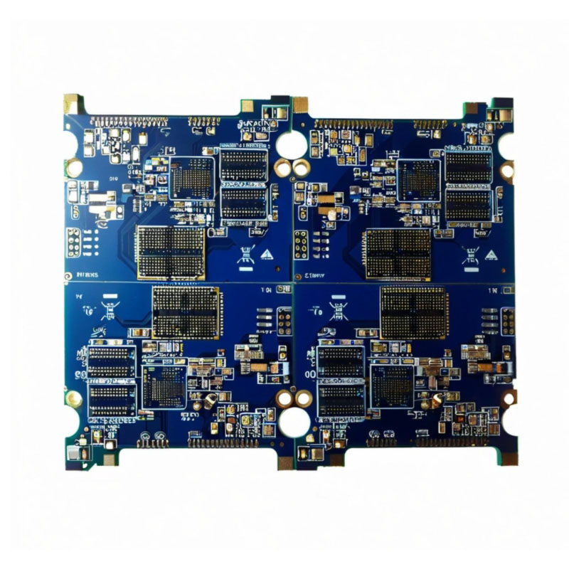
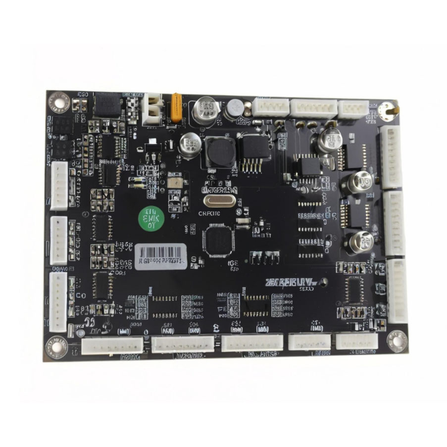
Experience grandiose innovation with our One-Stop Custom Prototype Circuit Board Design and PCBA Manufacture & Assembly Services. Enjoy exceptional markdown offers on fully customizable, RoHS-compliant solutions spanning reverse engineering and complex assembly (manual or automated SMT/DIP). We supply decorated, crowning circuit boards - rigid, flex, or rigid-flex - featuring 1-32 layers and tailored finishes. From quick prototyping (24 hours - 7 days) to scalable production (7-15 days), we accommodate bespoke needs in automotive, industrial, medical, and communication fields. Benefit from ESD-safe packaging, turnkey or consignment procurement, and vibrant color options.
Distinctive Features and Versatile Applications
Our one-stop supplier delivers customized PCBs and PCBA services with integrated reverse engineering, rapid prototyping, and decorated finishes. Special features include sensor switch availability, grandiose copper and board thickness range, extensive color choices, and both rigid and flex applications. Optimized for consumer electronics, automotive, medical, industrial, and communication environments, our solutions are crafted for diverse application media and site-specific requirements, ensuring durability, performance, and aesthetic value in every project.
Exceptional Offers, Payment Terms & Delivery
Leverage our markdown deals and lowest price offers on fully customized circuit board production. We provide sample availability to ensure confidence before your bulk order. With flexible payment terms and seamless transactions, orders are delivered efficiently through major FOB ports. Benefit from swift turnaround on prototypes and scheduled production deliveries, balancing cost-effectiveness and high-quality results for any project scale.
FAQ's of One stop Custom Prototype Circuit Board Design Reverse Engineering other PCB PCBA manufacture and assembly Service Supplier:
Q: How customizable are the PCB and PCBA services offered?
A: We provide extensive customization options, including Gerber, BOM, and schematic customization, board sizes up to 600mm x 1200mm, copper and board thickness, color, surface finish, and sensor switch integration to match your unique requirements.
Q: What is the standard process for reverse engineering a prototype circuit board?
A: Our reverse engineering process involves schematic extraction, BOM generation, and re-creation of Gerber files, ensuring seamless replication or improvement of legacy circuit boards for any application.
Q: When can I expect my prototype or production order to be delivered?
A: Prototyping lead times range from 24 hours to 7 days, while production orders are generally delivered within 7-15 days depending on quantity and customization details.
Q: What is the payment structure and do you offer samples?
A: Yes, we offer samples for evaluation before full-scale production. Flexible payment terms are available, and shipments are made via major FOB ports to accommodate global customers efficiently.
Q: Where can these customized PCBs be applied?
A: Our PCBs are grandiosely suited for consumer electronics, automotive, medical devices, industrial controls, and communication systems, meeting rigorous standards in site-specific and media-varied applications.

 Mon-Sat 9.00 AM to 6.00 PM





 Send Inquiry

 Send Inquiry
 Call Me Free


