


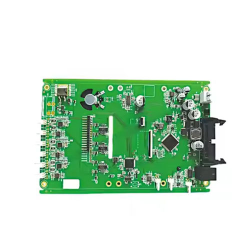
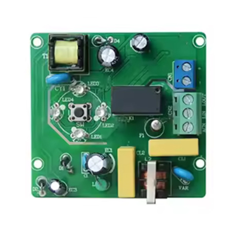
OEM Double-Sided PCB Prototype Service Custom PCBA Sample with High Quality Printing
Product Details:
- Test 100% E-test and AOI
- Min. Line Spacing 0.1 mm
- Hole Size Min 0.2mm
- Soldermask Green LPI
- Impedance 10% controlled impedance
- Insulation Resistance >10^12
- Flame Resistance Level UL94-V0
- Click to view more
X
OEM Double-Sided PCB Prototype Service Custom PCBA Sample with High Quality Printing Price And Quantity
- 100 Piece
- OEM/ODM
- 3-7 working days
- Yes
- Vacuum Sealed + ESD Bag
- SMT and Through-Hole Supported
- Available as per request
- -40°C to +130°C
- ±0.05 mm
- Gerber, BOM Accepted
- Consumer Electronics, Industrial Control, Telecom, Automotive
OEM Double-Sided PCB Prototype Service Custom PCBA Sample with High Quality Printing Product Specifications
- HASL/ENIG/OSP available
- 10% controlled impedance
- 220-440 Volt (V)
- >10^12
- Green
- Custom as per order
- 100% E-test and AOI
- White, high-resolution printing
- FR4
- Different available Millimeter (mm)
- UL94-V0
- 1-3 oz
- Min 0.2mm
- Optional integration
- 0.1 mm
- 2
- Double-Sided PCB
- Rigid
- 0.1 mm
- Customization available
- Yes
- Green LPI
- OEM/ODM
- 3-7 working days
- Yes
- Vacuum Sealed + ESD Bag
- SMT and Through-Hole Supported
- Available as per request
- -40°C to +130°C
- ±0.05 mm
- Gerber, BOM Accepted
- Consumer Electronics, Industrial Control, Telecom, Automotive
OEM Double-Sided PCB Prototype Service Custom PCBA Sample with High Quality Printing Trade Information
- Cash in Advance (CID)
- 5000 Piece Per Month
- 7 Days
- Asia, Australia, Central America, North America, South America, Eastern Europe, Western Europe, Middle East, Africa
Product Description
Experience the wondrous precision of our OEM Double-Sided PCB Prototype Service, delivering custom PCBA samples with matchless accuracy and majestic high-resolution printing. Redeem the benefits of instant checkout and swift prototype lead times-ephemeral waits of only 3-7 working days. Supporting both SMT and through-hole assembly, our service accommodates Gerber, BOM formats, and custom panel sizes. Enjoy flawless performance with 0.05 mm layer alignment, optional edge plating, and robust voltage endurance. Every board is vacuum-sealed, RoHS compliant, rigorously tested, and crafted to surpass industrial expectations-your gateway to next-level electronics.
Versatile Use & Application Guidance
OEM Double-Sided PCB Prototype Service is tailored for diverse sectors-consumer electronics, industrial control, telecom, and automotive. The majestic construction enables seamless application on rigid surfaces, supporting both SMT and through-hole mounted components. For best results, position the prototype on clean, flat surfaces, follow your schematic, and use within the recommended operating temperature. With optional sensor integration and customizable electrical components, this service matches a wide spectrum of product development directions.
Efficient Supply Chain & Secure Delivery
Our logistics-driven approach ensures instant checkout, quick dispatch, and reliable delivery of your custom PCB prototypes. With substantial supply ability, we process every purchase order swiftly. Vacuum-sealed packaging with ESD protection guarantees safe arrival, no matter your location. OEM/ODM support facilitates effortless integration into your workflow, ensuring your business always runs efficiently and ahead of schedule.
FAQ's of OEM Double-Sided PCB Prototype Service Custom PCBA Sample with High Quality Printing:
Q: How do I submit my design files for the PCB prototype service?
A: You can easily provide your design by submitting Gerber files and BOM during the order process. Our team will review and confirm compatibility before production begins.Q: What is the typical lead time for a custom double-sided PCB sample?
A: Our prototype lead time generally ranges from 3 to 7 working days, depending on the complexity and customization of your order.Q: Where can these PCBs be utilized most effectively?
A: These high-quality PCBs are ideal for use in consumer electronics, industrial control systems, telecommunications, and automotive applications, offering matchless reliability and adaptability.Q: What makes your PCB assembly process distinctive?
A: Our assembly supports both SMT and through-hole components, boasts 0.05 mm layer alignment, and utilizes 100% E-test and AOI for uncompromising quality and performance.Q: How are the PCBs packaged to ensure protection?
A: Each board is vacuum-sealed and placed in ESD bags, safeguarding it from static damage and contaminants during transit and storage.Q: What are the advantages of choosing this OEM/ODM PCB service?
A: You benefit from rapid lead times, high-resolution printing, robust customization options, and majestic quality assurance, helping accelerate your product development and time to market.Tell us about your requirement

Price:
Quantity
Select Unit
- 50
- 100
- 200
- 250
- 500
- 1000+
Additional detail
Mobile number
Email

Other Products in 'Double Sided PCBA' category
Contact Details
- No. 1506,15 Floor, SSG Tower, 561 ADien Bien Phu Str, Ward 25, Binh Thanh Dist, HCMC, Ho Chi Minh City - 717000, Thanh Pho Ho Chi Minh, Vietnam
- Ms. Yolanda Ke (Sales Account Manager)
- Mobile : +8613751081371
- Send Inquiry
NOVA TECHNOLOGY VIETNAMESE COMPANY LIMITED
|
 Call Me Free

NOVA TECHNOLOGY VIETNAMESE COMPANY LIMITED
All Rights Reserved.(Terms of Use)
Developed and Managed by Infocom Network Private Limited.
Developed and Managed by Infocom Network Private Limited.
