


Multilayer Pcb Specifications Pcba Assembly Manufacturer Competitive Price Wireless Charger Pcba
Product Details:
- Soldermask Green
- Min. Line Spacing 0.1mm
- Impedance Controlled Impedance
- Voltage Endurance 1500V AC/min
- Hole Size 0.2mm Min.
- Board Type Multilayer PCB
- Insulation Resistance >10^8
- Click to view more
X
Multilayer Pcb Specifications Pcba Assembly Manufacturer Competitive Price Wireless Charger Pcba Price And Quantity
- INR
- 1
- Qi Wireless Charging Compatible
- Anti-static Bag
- Wireless Charging Devices
- 7-12 Working Days
- Accepted
- 1 Piece
- Turnkey / Partial / Consigned
- SMT & Through Hole
- -20C to +70C
Multilayer Pcb Specifications Pcba Assembly Manufacturer Competitive Price Wireless Charger Pcba Product Specifications
- 0.1mm
- 1oz (35m)
- Green
- White
- 1500V AC/min
- Controlled Impedance
- Optional
- ENIG (Electroless Nickel/Immersion Gold)
- 1.6mm
- Green
- 94V-0
- High Quality Components
- 0.2mm Min.
- Multilayer PCB
- Wireless Charger PCBA
- >10^8
- 0.1mm
- 4 Layers
- Flying Probe / E-test
- Customized
- FR4
- Qi Wireless Charging Compatible
- Anti-static Bag
- Wireless Charging Devices
- 7-12 Working Days
- Accepted
- 1 Piece
- Turnkey / Partial / Consigned
- SMT & Through Hole
- -20C to +70C
Product Description
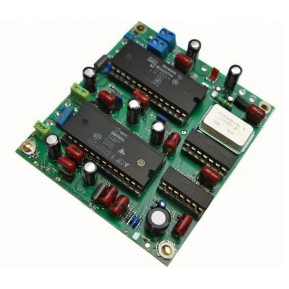
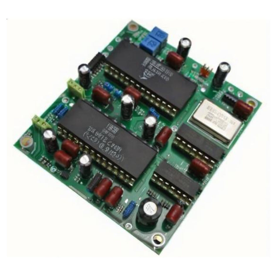
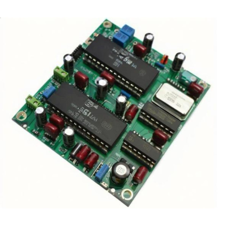
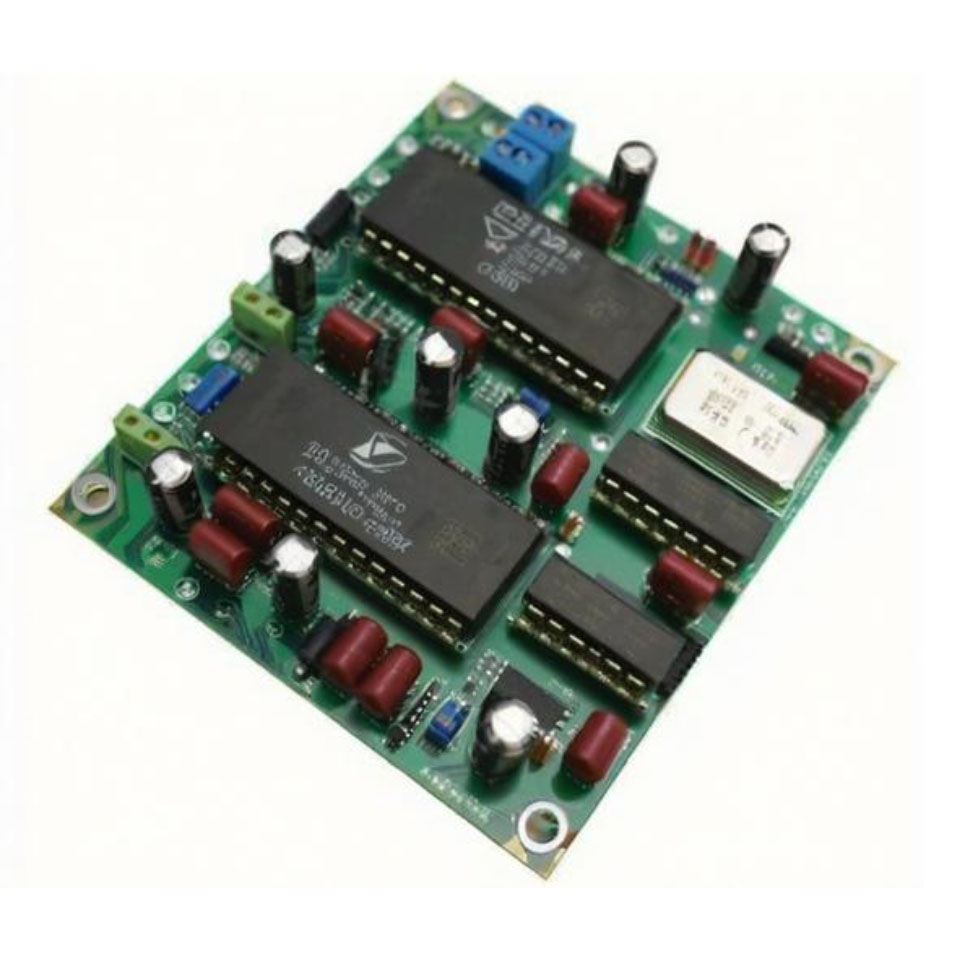
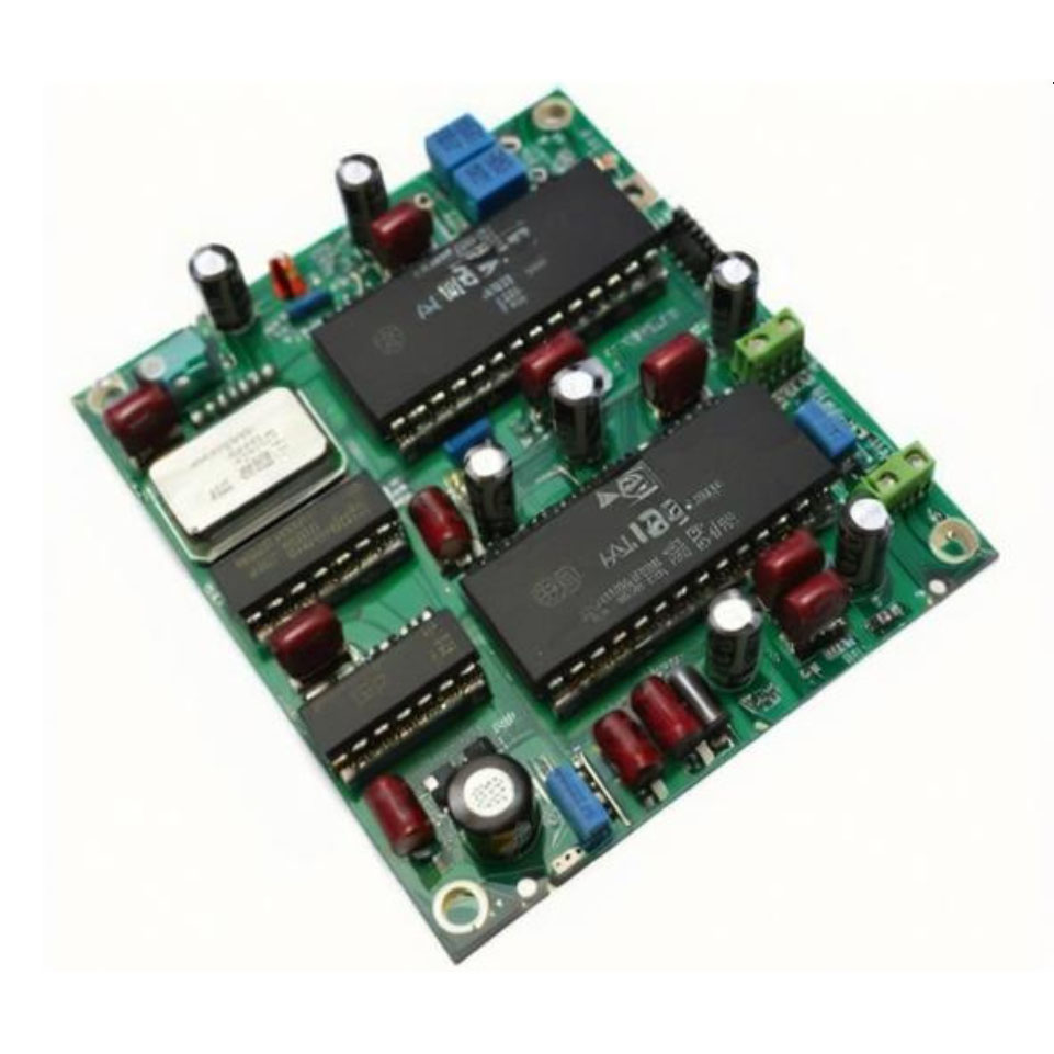
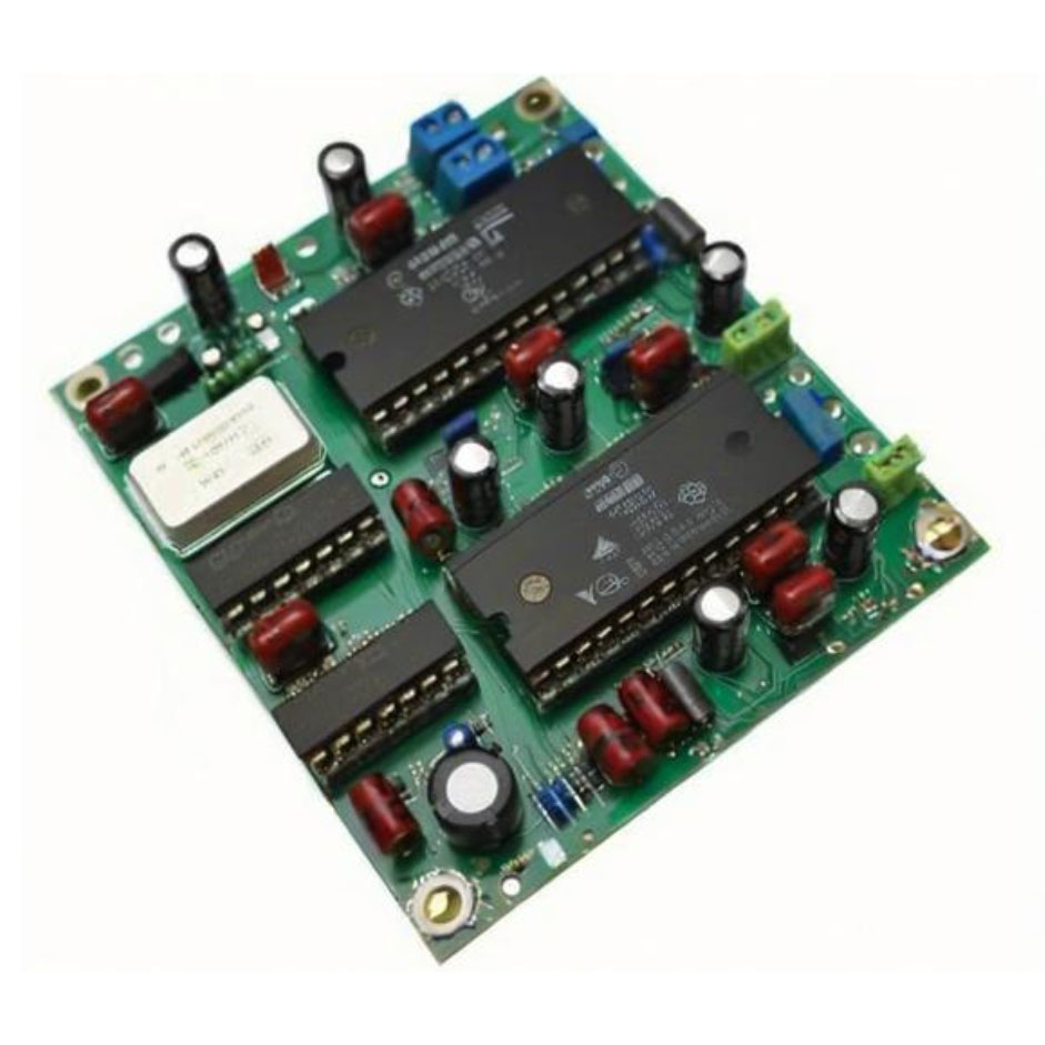
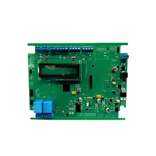
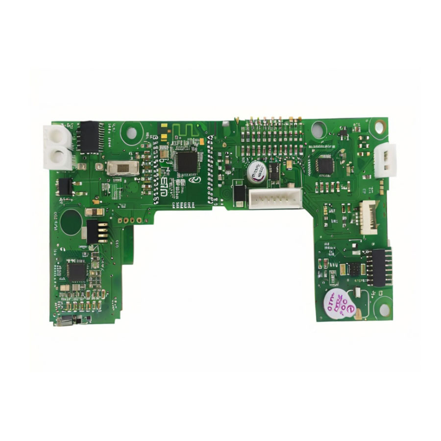
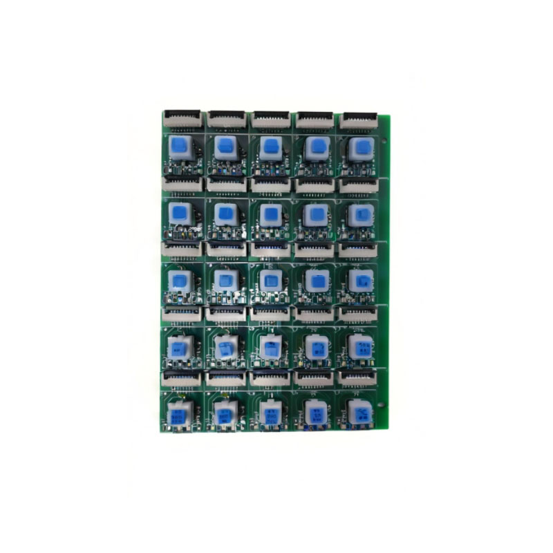
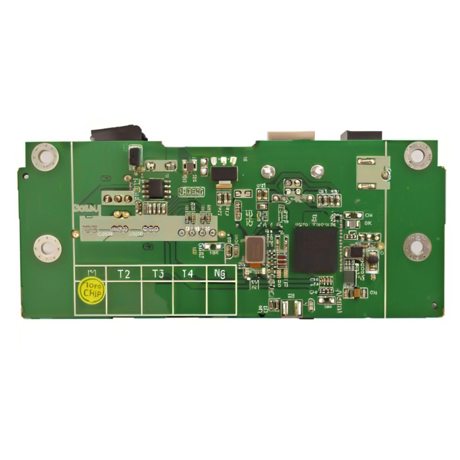
Select this splendid Multilayer PCB Specifications PCBA Assembly Manufacturer for your wireless charger needs and utilise our unrivaled offer. Enjoy a majestic balance of premium-quality manufacturing and competitive price. Featuring 4 layers, ENIG surface finish, and FR4 base material, this product ensures superior durability and excellent insulation resistance (>10^8). With custom panel sizes and OEM/ODM service accepted, we provide a low MOQ of just 1 piece and fast lead times-7-12 working days. Component sourcing is flexible-turnkey, partial, or consigned. Trust us for anti-static packing, controlled impedance, and rigorous quality tests. Discount available for bulk orders.
Wireless Charger PCBA: Application Method and Utilisation
This multilayer PCBA is expertly designed for integration into wireless charging devices. Application is seamless-simply select the appropriate customized panel size and assemble it into your device. The surface is protected with an ENIG finish and a resilient green solder mask, ensuring reliable performance and durability. Perfect for consumer electronics, its high compatibility with Qi wireless charging standards enhances its usage in diverse environments, from offices to homes. Utilise this solution for next-generation wireless device efficiency.
Certifications, FOB Port, and Premium Dispatching
Our Multilayer PCB Assemblies come with certifications attesting to high-quality standards. Each unit is inspected and dispatched promptly from India through leading FOB ports, ensuring swift shipment to your destination. Every PCBA is securely packed in premium anti-static bags to maintain product integrity throughout transit. Orders are handled with utmost care, guaranteeing a reliable supply chain experience from dispatching to final shipment. Select us for certified and premium wireless charger PCBAs shipped on time, every time.
FAQ's of Multilayer Pcb Specifications Pcba Assembly Manufacturer Competitive Price Wireless Charger Pcba:
Q: How does the assembly process work for this multilayer wireless charger PCBA?
A: Our assembly process includes both SMT and Through Hole assembly, utilising advanced technology for mounting electrical components. We offer flexible sourcing-turnkey, partial, or consigned-based on your needs. Every PCBA is thoroughly tested with Flying Probe or E-tests before shipment.Q: What are the main applications of this wireless charger PCBA?
A: This product is primarily used in wireless charging devices. Its Qi wireless charging compatibility makes it ideal for integration into consumer electronics requiring efficient, cable-free charging solutions.Q: When can I expect delivery after placing an order?
A: Your PCBA order will be dispatched within a lead time of 7-12 working days. Shipment is expedited from major Indian FOB ports, ensuring swift delivery to your designated location.Q: Where are these wireless charger PCBAs manufactured and can I request OEM/ODM service?
A: All wireless charger PCBAs are manufactured in state-of-the-art facilities in India. We accept OEM and ODM orders, allowing for complete customization to your project specifications.Q: What benefit does the ENIG surface finish provide?
A: The ENIG (Electroless Nickel/Immersion Gold) finish ensures excellent corrosion resistance, superior solderability, and long-lasting surface durability-ideal for high-reliability applications in wireless charging devices.Q: How is the product packaged to ensure safety during transit?
A: Each board is packed in premium anti-static bags to prevent electrostatic damage. Additional secure packaging ensures the PCBA arrives in optimal condition, ready for integration.Tell us about your requirement

Price:
Quantity
Select Unit
- 50
- 100
- 200
- 250
- 500
- 1000+
Additional detail
Mobile number
Email

Other Products in 'Multilayer PCBA' category
Contact Details
- No. 1506,15 Floor, SSG Tower, 561 ADien Bien Phu Str, Ward 25, Binh Thanh Dist, HCMC, Ho Chi Minh City - 717000, Thanh Pho Ho Chi Minh, Vietnam
- Ms. Yolanda Ke (Sales Account Manager)
- Mobile : +8613751081371
- Send Inquiry
NOVA TECHNOLOGY VIETNAMESE COMPANY LIMITED
|


NOVA TECHNOLOGY VIETNAMESE COMPANY LIMITED
All Rights Reserved.(Terms of Use)
Developed and Managed by Infocom Network Private Limited.
Developed and Managed by Infocom Network Private Limited.
