


High Quality OEM HDI PCB Manufacturing China Leader Company Specializing in PCBA Design and Manufacture
Product Details:
- Hole Size Min. 0.1mm (Laser Drilled)
- Test 100% E-test, AOI, X-ray, Functional Test
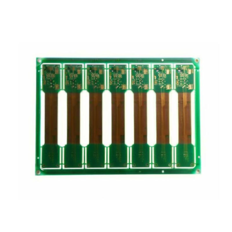
- Board Type Rigid, Rigid-Flex, Flex
- Impedance Controlled within 10%
- Soldermask Green, Blue, Black, White, Red, Yellow (customizable)
- Insulation Resistance >10^12
- Min. Line Spacing 0.05mm
- Click to view more
X
High Quality OEM HDI PCB Manufacturing China Leader Company Specializing in PCBA Design and Manufacture Price And Quantity
- INR
- 1
- Nickel/Gold, Electrolytic or Electroless (per finish)
- 10% or per IPC Standard
- Up to 260C (lead-free process compatible)
- 50m
- Customized vacuum and anti-static packaging
- Full PCBA, Schematic and Layout design support
- No MOQ, prototype to mass production
High Quality OEM HDI PCB Manufacturing China Leader Company Specializing in PCBA Design and Manufacture Product Specifications
- SMT, Through Hole, BGA, QFN, POP, CSP, Fine Pitch IC
- >1500V
- Controlled within 10%
- up to 600mm x 1200mm
- 100% E-test, AOI, X-ray, Functional Test
- Min. 0.1mm (Laser Drilled)
- 0.5oz - 2oz (customizable)
- Rigid, Rigid-Flex, Flex
- FR-4, Rogers, High Tg, Halogen-Free, CEM-3, Polyimide
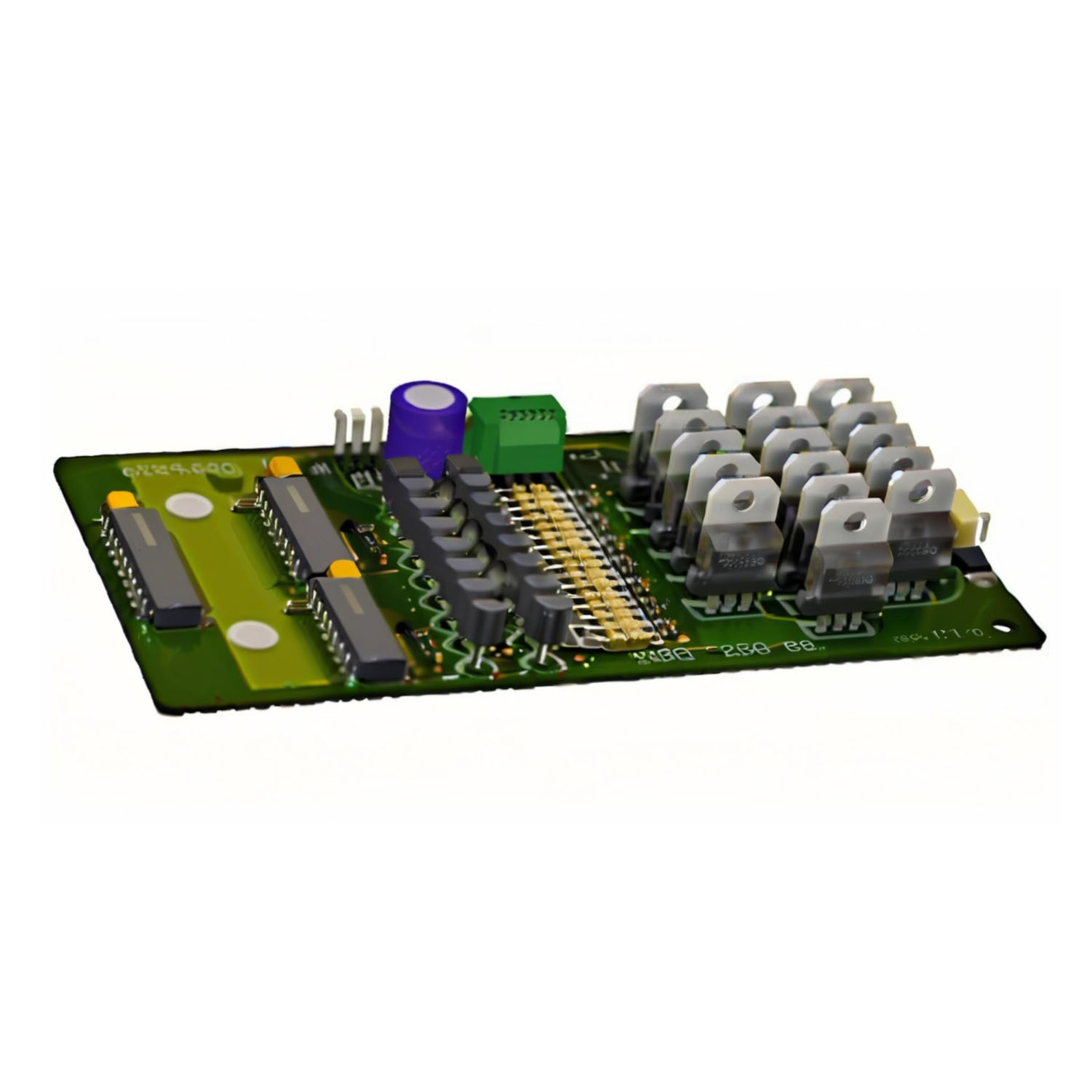
- HDI PCB (High Density Interconnect Printed Circuit Board)
- 0.05mm
- 0.4mm - 3.2mm
- 2-20 Layers
- Optional integration (per customer design)
- ENIG, HASL, OSP, Immersion Silver, Immersion Tin, Gold Finger
- White, Yellow (customizable)
- Green, Blue, Red, Black, White (customizable)
- UL94 V-0
- 0.05mm
- >10^12
- Green, Blue, Black, White, Red, Yellow (customizable)
- Nickel/Gold, Electrolytic or Electroless (per finish)
- 10% or per IPC Standard
- Up to 260C (lead-free process compatible)
- 50m
- Customized vacuum and anti-static packaging
- Full PCBA, Schematic and Layout design support
- No MOQ, prototype to mass production
Product Description
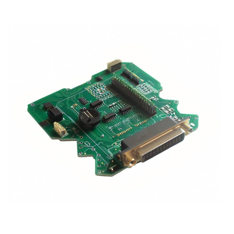
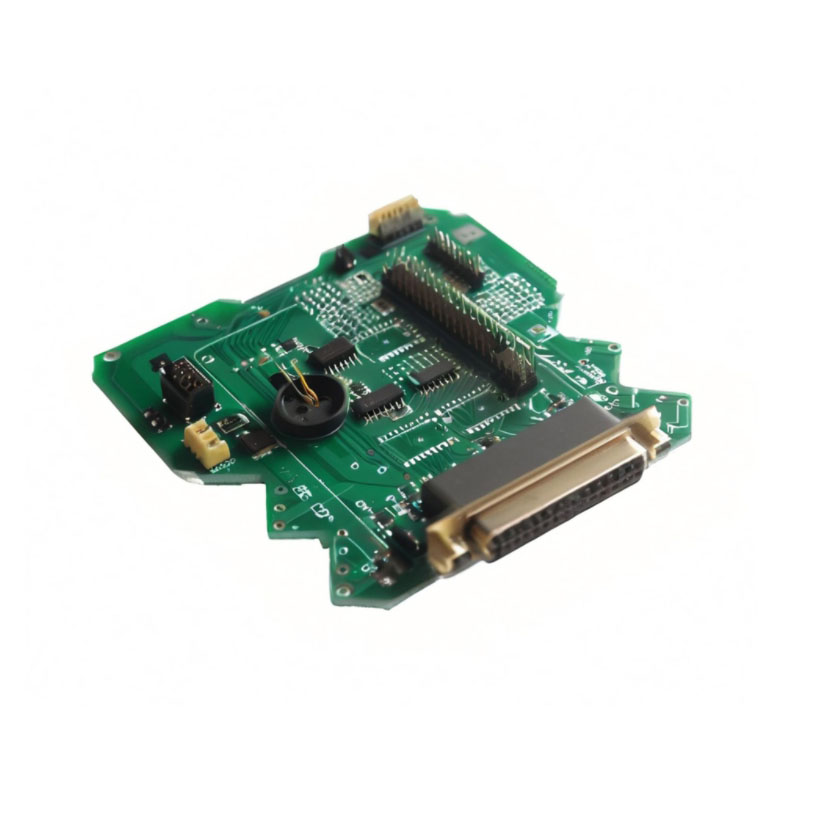
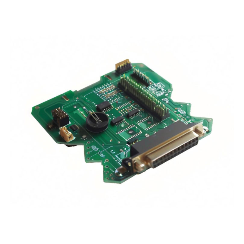
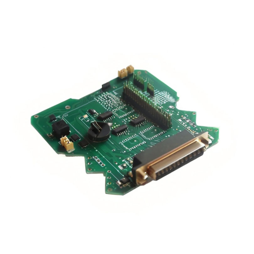
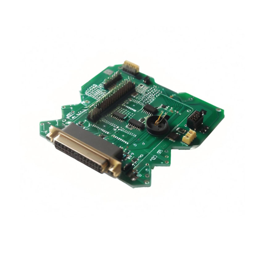
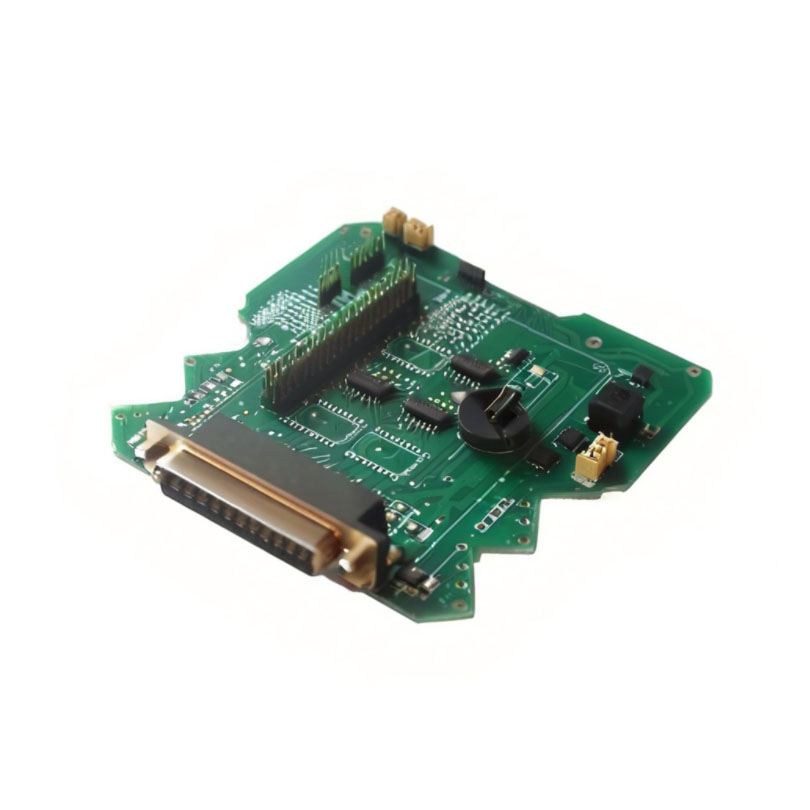
Commanding the advanced electronics landscape, our High Quality OEM HDI PCB Manufacturing China Leader delivers enviable precision in PCBA design and fabrication. Redeem enviable benefits with our max finished panel thickness tolerance of 10%, robust up to 260C for lead-free processes, and impeccable layer alignment at 50m. Enjoy enlightened design services from schematic to layout, utilizing nickel/gold plating (electrolytic/electroless). No MOQ enables seamless reservation of prototype or mass production. Clearance opportunities available! Our tailored OEM solutions bring an elevated standard to global exporters, manufacturers, and suppliers in India.
Application Surface & Competitive Advantages
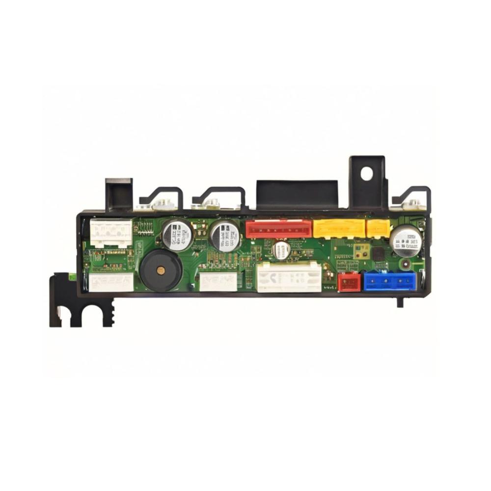
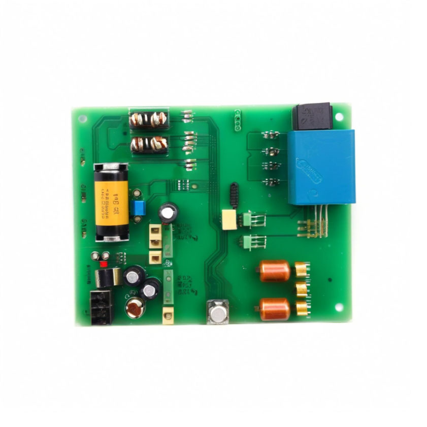
Our HDI PCB solutions deliver extraordinary reliability across automotive, communication, medical, and industrial applications. The surface of application extends to complex circuitry and high-density connectors, meeting demanding project criteria. Our competitive advantages include tight tolerances, customizable plating, controlled impedance, and optional sensor switch integration. We guarantee robust performance through advanced testing (E-test, AOI, X-ray, functional), backing your product's commanding market presence with superior technical support and rapid turnaround times.
Sample, Certifications & Logistics Details
Sample PCBs can be reserved and are available for clearance and evaluation prior to mass orders. Every order is backed by internationally recognized certifications, ensuring compliance and quality assurance. Products are efficiently dispatched from our China facility via major FOB ports, with logistics optimized for swift delivery. Our streamlined process enables clients to benefit from reliable freight arrangements and tracking, ensuring your production timelines are met with precision and care.
Application Surface & Competitive Advantages
Our HDI PCB solutions deliver extraordinary reliability across automotive, communication, medical, and industrial applications. The surface of application extends to complex circuitry and high-density connectors, meeting demanding project criteria. Our competitive advantages include tight tolerances, customizable plating, controlled impedance, and optional sensor switch integration. We guarantee robust performance through advanced testing (E-test, AOI, X-ray, functional), backing your product's commanding market presence with superior technical support and rapid turnaround times.
Sample, Certifications & Logistics Details
Sample PCBs can be reserved and are available for clearance and evaluation prior to mass orders. Every order is backed by internationally recognized certifications, ensuring compliance and quality assurance. Products are efficiently dispatched from our China facility via major FOB ports, with logistics optimized for swift delivery. Our streamlined process enables clients to benefit from reliable freight arrangements and tracking, ensuring your production timelines are met with precision and care.
FAQ's of High Quality OEM HDI PCB Manufacturing China Leader Company Specializing in PCBA Design and Manufacture:
Q: How can I reserve a prototype or place a bulk order for HDI PCBs?
A: You can easily reserve prototypes or redeem bulk orders through our official website or by contacting our sales team. We accept projects of all sizes with no minimum order quantity (MOQ), ensuring flexibility from prototype runs to full-scale manufacturing.Q: What surface finishes and plating options do you offer for PCB manufacturing?
A: We provide a commanding range of surface finishes such as ENIG, HASL, OSP, Immersion Silver, Immersion Tin, and Gold Finger. Plating is available as nickel/gold, either electrolytic or electroless, customized for your application needs.Q: What is the maximum working temperature and tolerance specifications for your PCBs?
A: Our high quality HDI PCBs can withstand working temperatures up to 260C (compatible with lead-free processes), offering a finished panel thickness tolerance of 10% (or IPC standard) and layer alignment tolerance of 50m, ensuring enviable reliability.Q: Where are your products shipped from and what logistics services are provided?
A: All orders are dispatched from our China manufacturing facility. We offer FOB port shipment with robust freight solutions, ensuring timely logistics management and traceability throughout the delivery process.Q: What certifications and quality tests are performed on your PCB products?
A: Every PCB undergoes 100% electrical (E-test), AOI, X-ray, and functional testing. Our manufacturing follows global certification standards, providing guaranteed quality, flame resistance (UL94 V-0), and high insulation resistance (>10^12), ensuring your peace of mind.Q: When are sample PCBs available for inspection before ordering?
A: Sample PCBs are available upon request and can be reserved to verify quality and compliance with your requirements before proceeding with mass production.Tell us about your requirement

Price:
Quantity
Select Unit
- 50
- 100
- 200
- 250
- 500
- 1000+
Additional detail
Mobile number
Email

Other Products in 'PCBA Customized' category
Contact Details
- No. 1506,15 Floor, SSG Tower, 561 ADien Bien Phu Str, Ward 25, Binh Thanh Dist, HCMC, Ho Chi Minh City - 717000, Thanh Pho Ho Chi Minh, Vietnam
- Ms. Yolanda Ke (Sales Account Manager)
- Mobile : +8613751081371
- Send Inquiry
NOVA TECHNOLOGY VIETNAMESE COMPANY LIMITED
|
 Call Me Free

NOVA TECHNOLOGY VIETNAMESE COMPANY LIMITED
All Rights Reserved.(Terms of Use)
Developed and Managed by Infocom Network Private Limited.
Developed and Managed by Infocom Network Private Limited.
