


Printed Circuit Board Buried & Blind via PCB HDI High Layer PCB and 8 Layer Board Control Impedance Board
1.0 आईएनआर
उत्पाद विवरण:
- छेद का आकार 0.25mm (Typical for vias)
- प्रतिबाधा Controlled Impedance
- टेस्ट
- न्यूनतम। लाइन की चौड़ाई 0.075mm
- बोर्ड का प्रकार
- ज्वाला प्रतिरोध स्तर V-0
- इन्सुलेशन प्रतिरोध 100MΩ
- Click to view more
X
मूल्य और मात्रा
- 1
उत्पाद की विशेषताएं
- None
- 0.25mm (Typical for vias)
- 1.6mm
- Integrated circuitry and connectors
- 0.075mm
- Controlled Impedance
- 100MΩ
- 1 Year
- 1oz Copper
- 0.075mm
- 300V
- Printed Circuit Board
- V-0
- 300mm x 500mm
उत्पाद विवरण
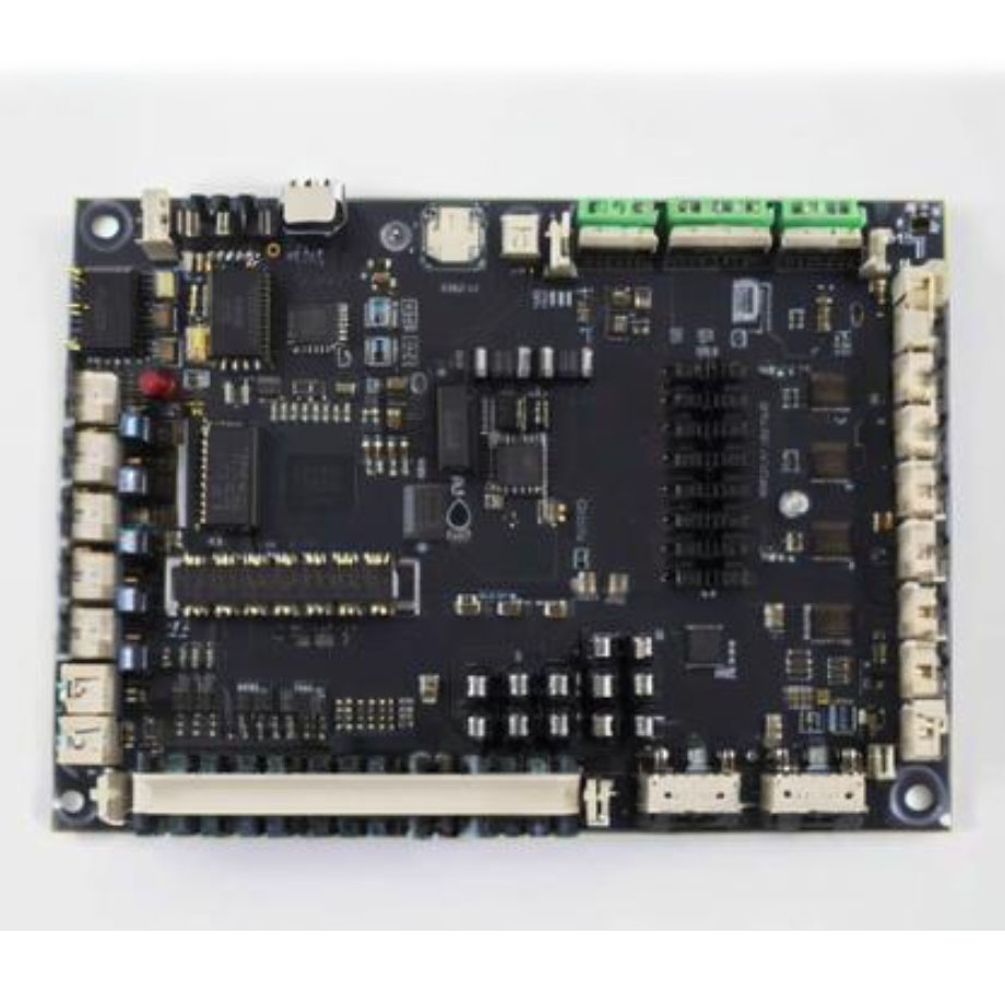
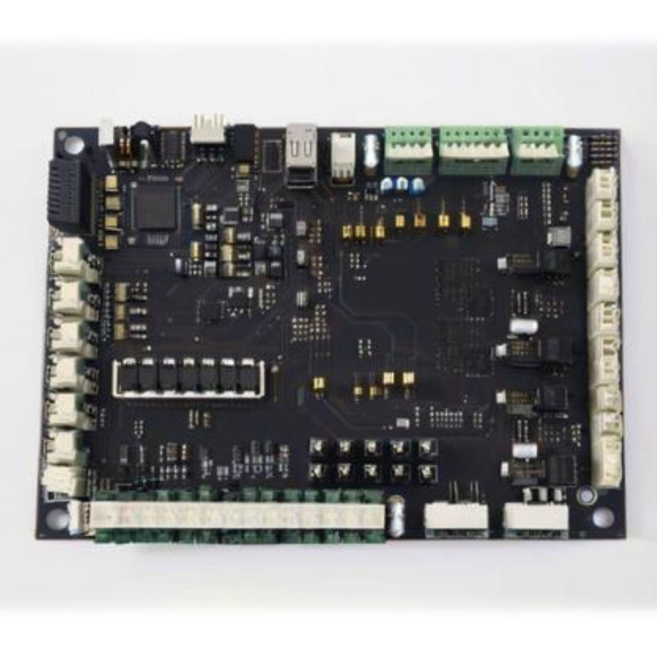
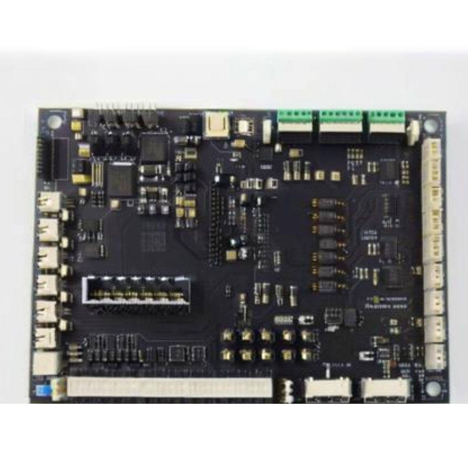
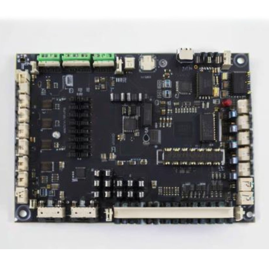
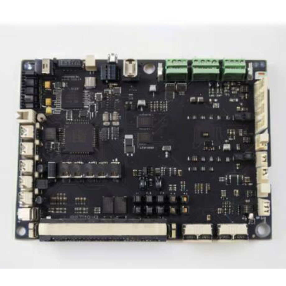
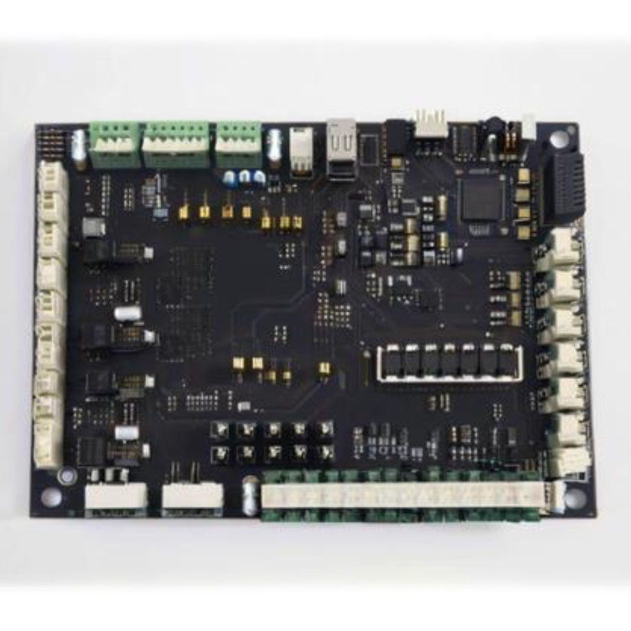
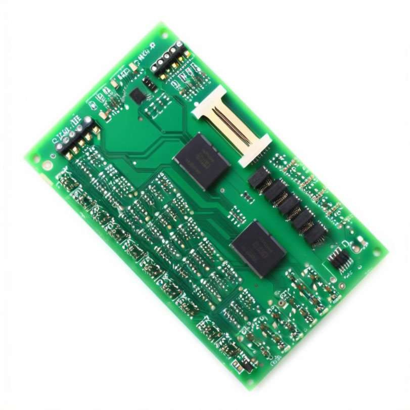
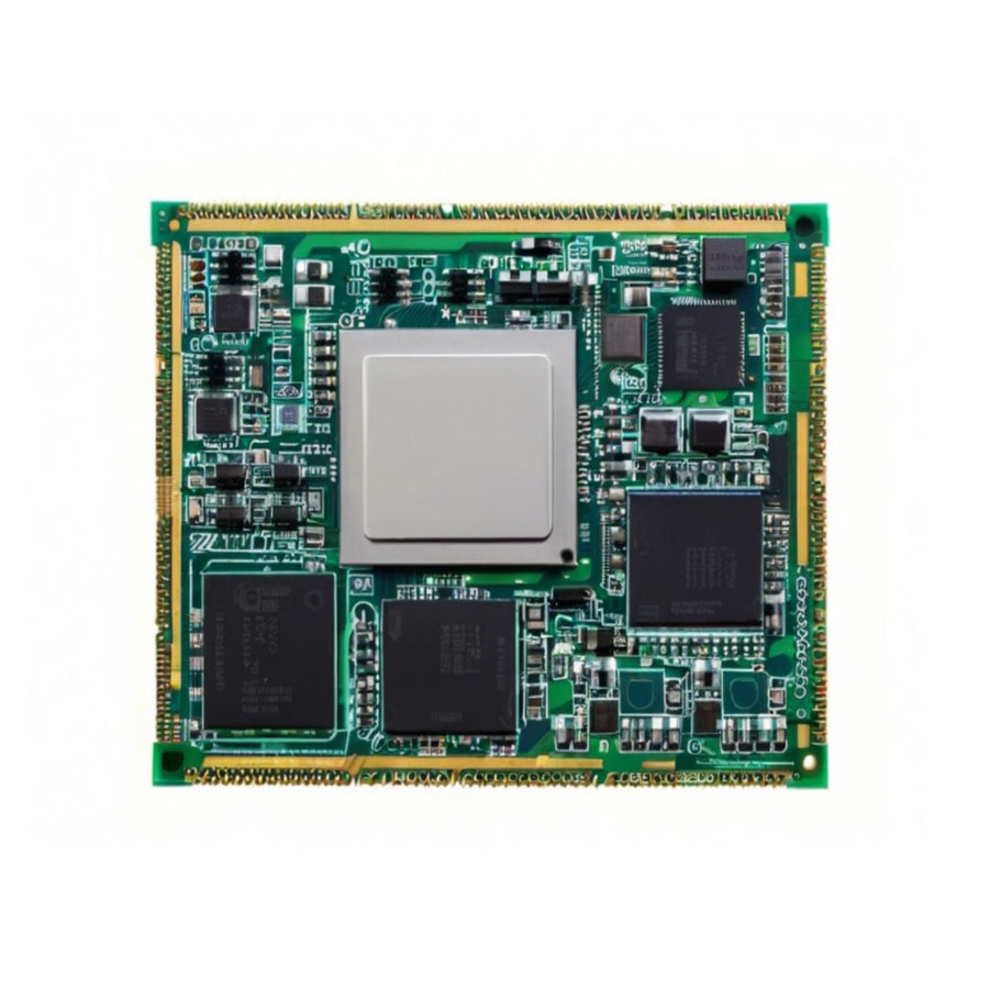
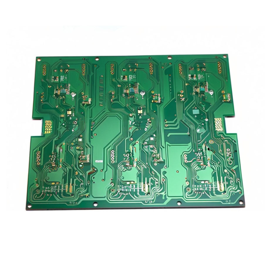
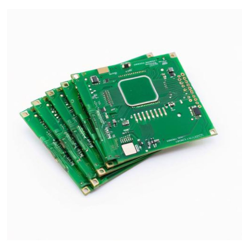
Introducing the latest in PCB innovationour Lavish Printed Circuit Board Buried & Blind via HDI High Layer Design. Exquisitely crafted with integrated circuitry and connectors, this valorous 8-layer board features highlighted attributes such as 1oz copper thickness, a robust FR4 base material, and a rich black ENIG surface finish. With limited stock available, it offers flame resistance of V-0 and controlled impedance, making it ideal for high-reliability applications. Each board comes with a 1-year warranty, ensuring premium performance and peace of mind.
Advanced Applications and Machine Features
The Printed Circuit Board Buried & Blind via PCB8 Layer HDI Control Impedance Board stands out for its versatile application surface. Designed for cutting-edge electronics, its highlighted features include a pioneering ENIG surface, high insulation resistance, and precise line capability. Built for valorous operation, this board suits industrial, automotive, and communication equipment. Its exquisite finish and robust build ensure lasting functionality for rigorous usage across critical domains.
Market Value and Export Capabilities
With an established presence in both domestic and global markets, this PCB solution brings considerable market value. Samples are available upon inquiry to assess performance before major expenditure decisions. The supply ability meets significant export volumes, making it a prime choice for extensive industrial needs. With efficient distribution channels and a commitment to quality, this board reinforces our reputation as a reliable exporter, manufacturer, and supplier worldwide.
FAQs of Printed Circuit Board Buried & Blind via PCB HDI High Layer PCB and 8 Layer Board Control Impedance Board:
Q: How does the blind and buried via structure benefit PCB performance?
A: Blind and buried vias reduce space and layer count, ensuring higher routing density and improved signal integrity in compact designs.Q: What features make this 8-layer HDI board suitable for advanced electronics?
A: Key features include controlled impedance, 1oz copper thickness, ENIG surface finish, and high V-0 flame resistance, making it ideal for high-performance electronic systems.Q: When is it recommended to use a board with controlled impedance?
A: Controlled impedance boards are essential when signal integrity is critical, such as in high-speed communication or signal processing equipment.Q: Where can customers request a sample of this PCB?
A: Samples are available upon inquiry through our sales channel, allowing clients to evaluate the products quality and suitability before large-scale orders.Q: What process ensures the reliability of these PCBs?
A: Every board undergoes flying probe testing, confirming electrical reliability and fault-free performance prior to shipment.Q: What are the main export markets for this PCB product?
A: Our products are exported to a range of regions, including North America, Europe, and select Asian markets, consistently meeting industry standards worldwide.Tell us about your requirement

Price: Â
Quantity
Select Unit
- 50
- 100
- 200
- 250
- 500
- 1000+
Additional detail
मोबाइल number
Email

मल्टीलेयर पीसीबीए अन्य उत्पाद
सम्पर्क करने का विवरण
- नंबर 1506,15 मंजिल, एसएसजी टॉवर, 561 एडीएन बिएन फु स्ट्रीट, वार्ड 25, बिन्ह थान जिला, एचसीएमसी,हो ची मिन्ह सिटी - 717000, थान्ह फो हो ची मिन्ह, वियतनाम
- सुश्री टिफ़नी (थाओ गुयेन) (बिक्री खाता प्रबंधक)
- मोबाइल : +8613751081371
- जांच भेजें
नोवा टेक्नोलॉजी वियतनामी कंपनी लिमिटेड
|


NOVA TECHNOLOGY VIETNAMESE COMPANY LIMITED
सर्वाधिकार सुरक्षित.(उपयोग की शर्तें)
इन्फोकॉम नेटवर्क प्राइवेट लिमिटेड . द्वारा विकसित एवं प्रबंधित
इन्फोकॉम नेटवर्क प्राइवेट लिमिटेड . द्वारा विकसित एवं प्रबंधित
