


PCBA Professional Design Custom Electronic Multi-Layer Printed Circuit Board PCB And PCBA Manufacturers one-stop service
उत्पाद विवरण:
- न्यूनतम। लाइन की चौड़ाई 3mil (0.075mm)
- प्रतिबाधा 10% controlled impedance
- बोर्ड का प्रकार
- वोल्टेज एंड्योरेंस >1500V
- सिल्कस्क्रीन
- न्यूनतम। लाइन स्पेसिंग 3mil (0.075mm)
- ज्वाला प्रतिरोध स्तर V0 (UL94V-0)
- Click to view more
X
मूल्य और मात्रा
- 1
- आईएनआर
- Vacuum Packing, Carton
- 610mm x 1200mm
- 100% E-Test and Optical Inspection
- Turnkey/Partial Turnkey/BOM Service
- Available
- One-stop PCB & PCBA Manufacturing
- 7-15 working days
उत्पाद की विशेषताएं
- Through-Hole, SMD, BGA, QFN, and Others
- 10% controlled impedance
- >10^12
- Min 0.15mm
- 3mil (0.075mm)
- 3mil (0.075mm)
- V0 (UL94V-0)
- 1oz, 2oz, 3oz, 4oz
- >1500V
- Custom Integration
- 0.4mm-3.2mm
- Customizable/As required
- Multi-Layer PCB & PCBA
- Vacuum Packing, Carton
- 610mm x 1200mm
- 100% E-Test and Optical Inspection
- Turnkey/Partial Turnkey/BOM Service
- Available
- One-stop PCB & PCBA Manufacturing
- 7-15 working days
उत्पाद विवरण
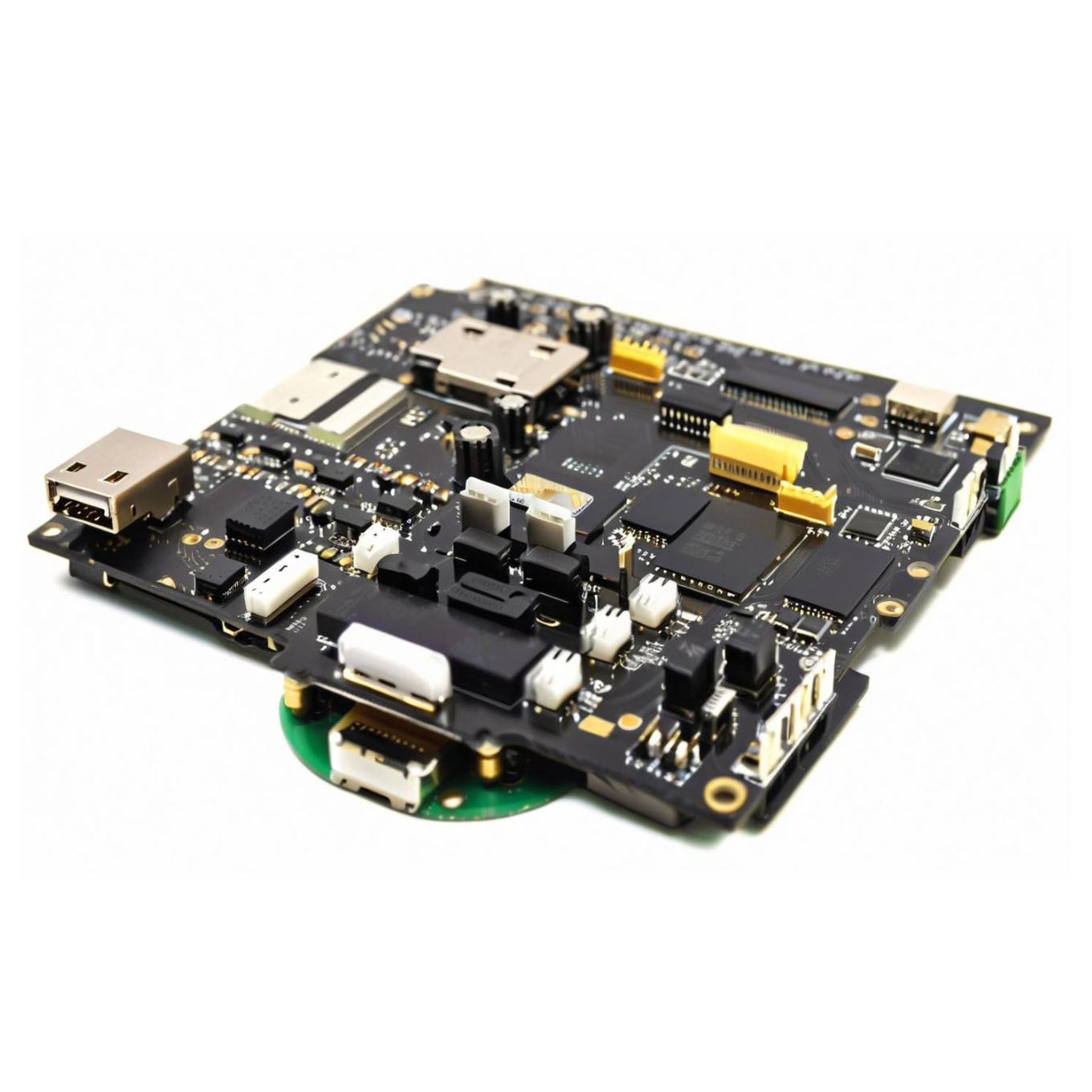
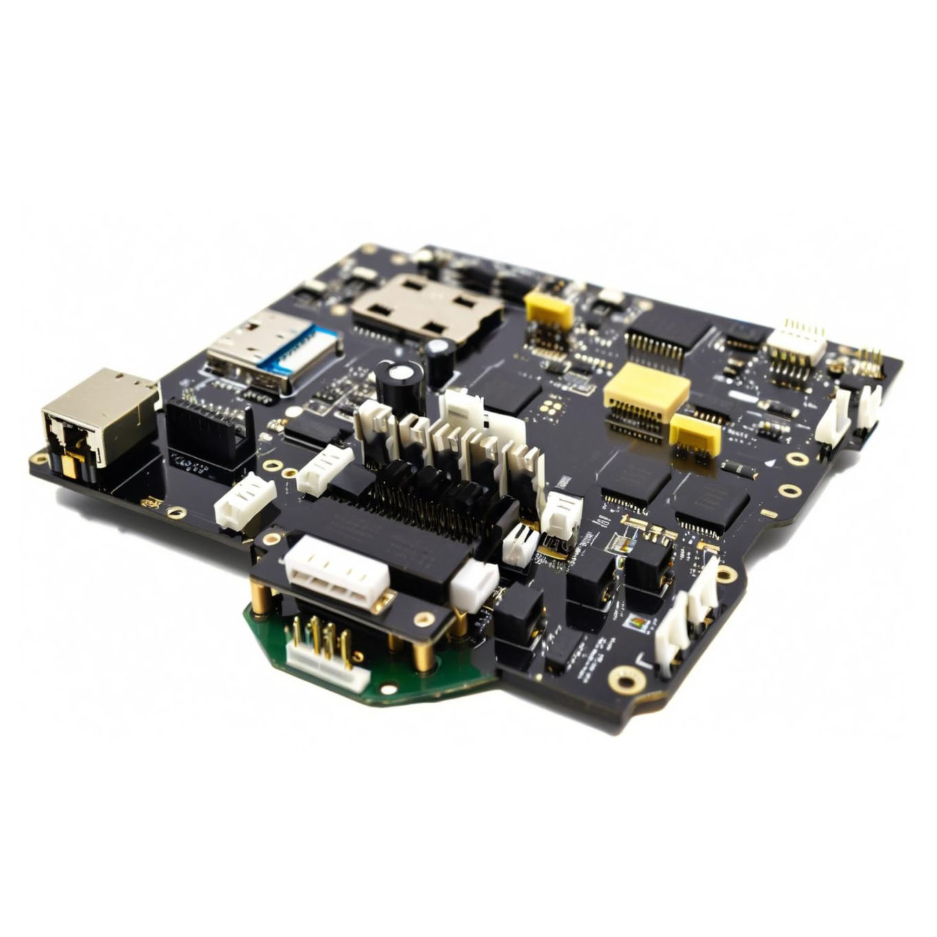
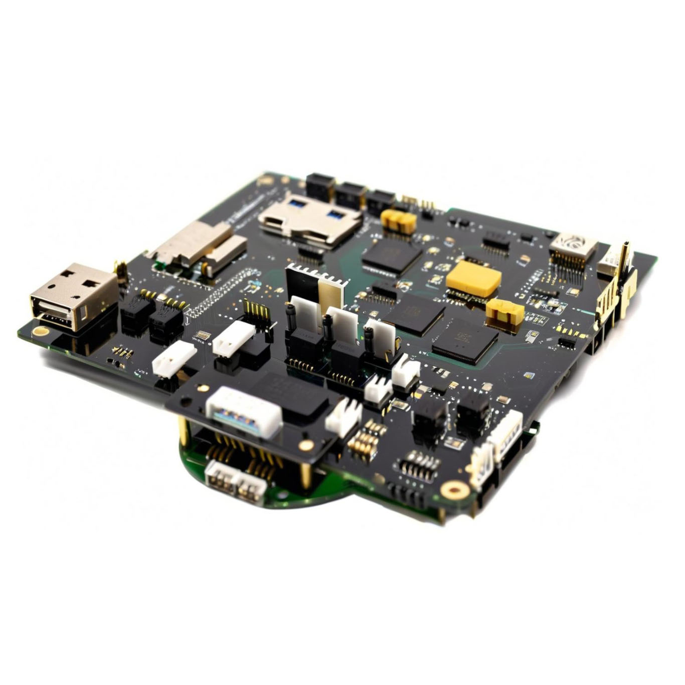
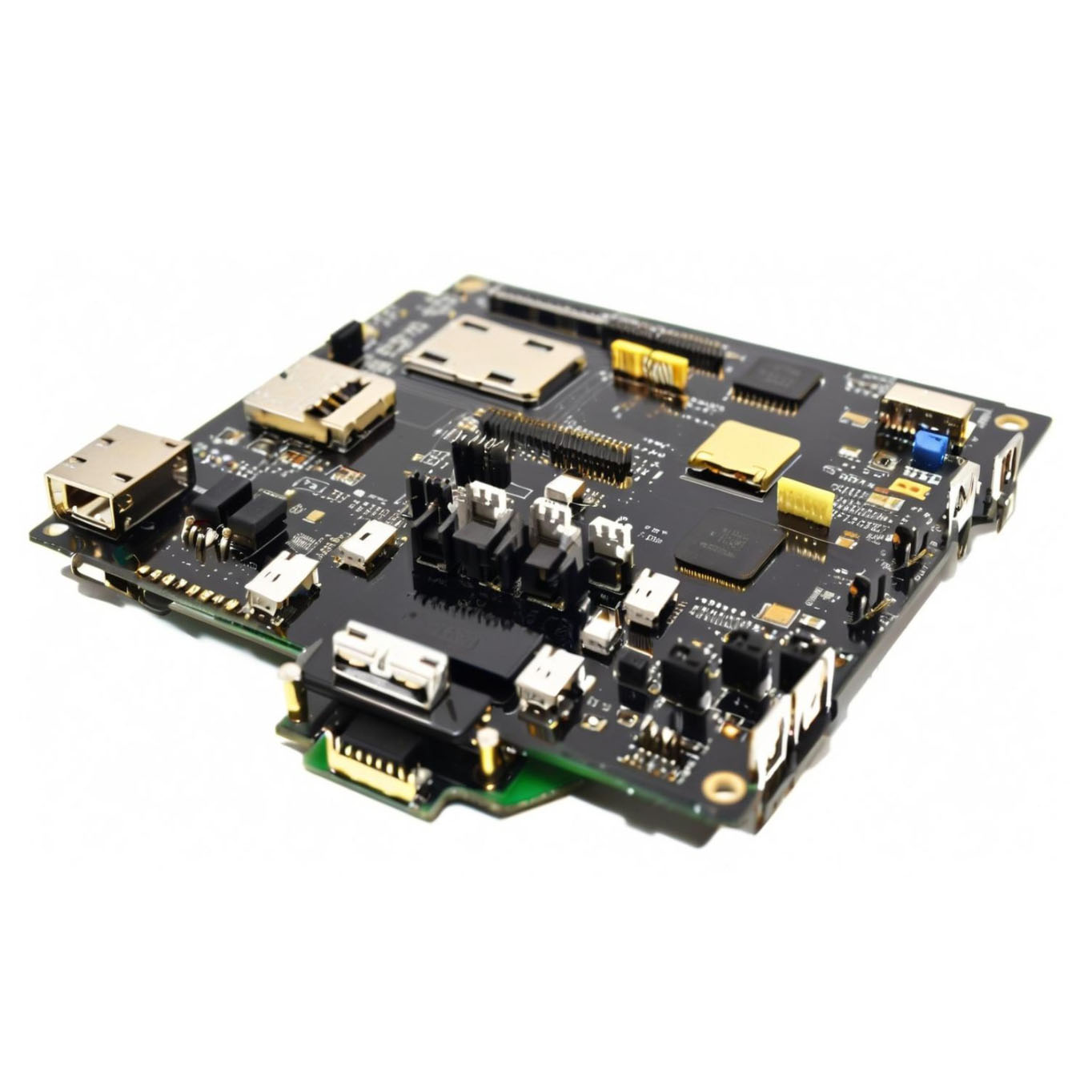
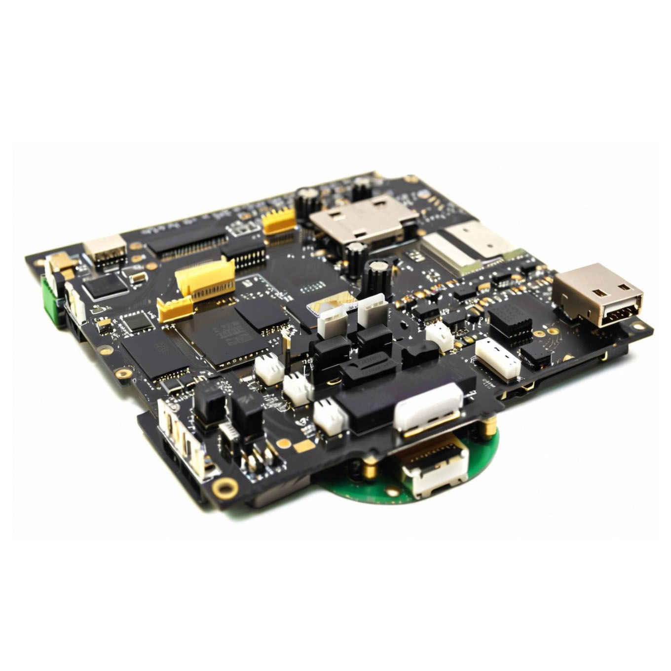
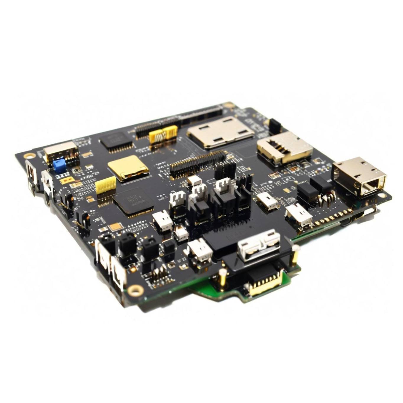
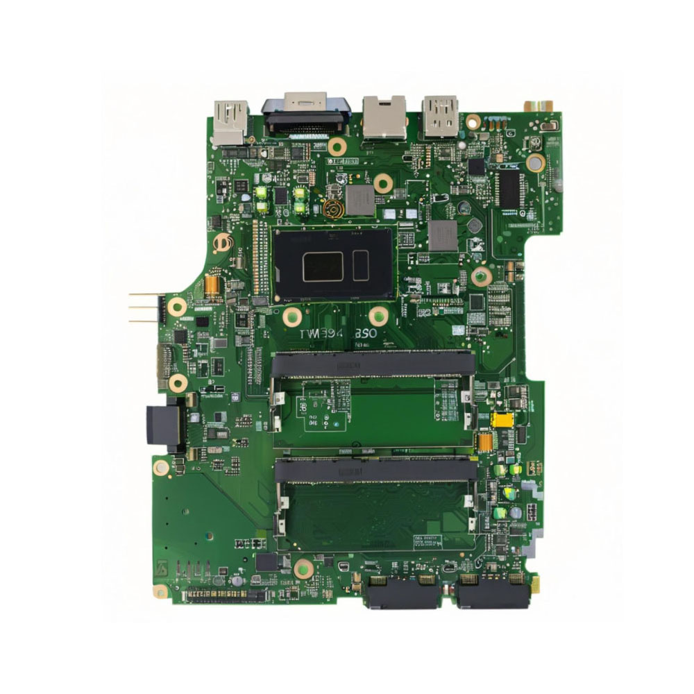
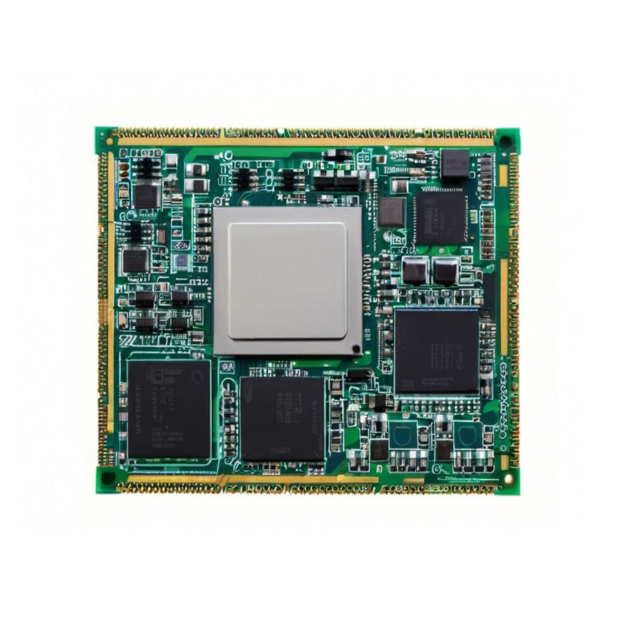
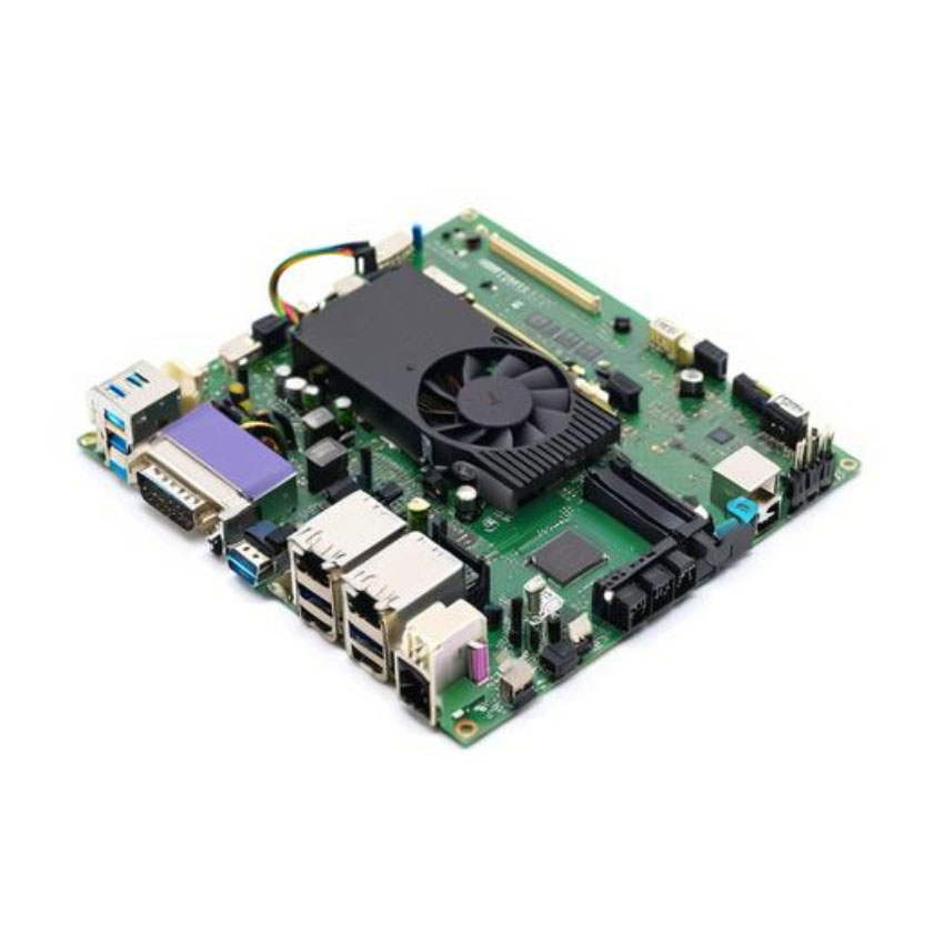
Reserve your spot with our PCBA Professional Design and Custom Electronic Multi-Layer PCB solutions, offering prodigious one-stop service for assembly, forging a radiant standard in performance and reliability. Noble in capability with 2-24 layers, our kingly manufacturing suite highlights rapid 7-15 day lead times, component sourcing flexibility, and advanced customization. Redeem superior quality with copper thickness up to 4oz, 610mm x 1200mm board sizes, and 100% E-Test and optical inspections. From prototype to production, we illuminate your innovation journey, supporting OEM/ODM needs, and exporting across India and beyond.
Applications, Advantages, and Areas of Use
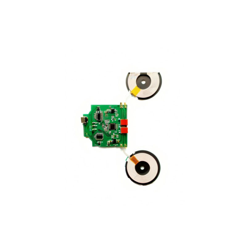
Our highlighted PCBA and multi-layer PCB solutions serve a broad spectrum: from industrial controls to consumer electronics, IoT devices, and automotive electronics. The radiant advantages include swift lead times, customizable panel sizes, and robust quality assurance. Surface finishes such as ENIG, gold plating, and OSP ensure reliability under demanding conditions. Advanced integration like sensor switches and varied board colors make our service kingly for R&D, startups, and large-scale manufacturers alike.
Sample Policy, Export Markets & Certifications
Proposal amount for sampling depends on project complexity; sample Exchange is streamlined and efficient. Packing & Dispatch is meticulously managed in vacuum-sealed and robust cartons, ensuring products arrive protected. We cater to main export markets including India, Southeast Asia, and regions globally. Our certifications and adherence to industry standards guarantee every delivery meets prodigious quality and safety expectations.
Applications, Advantages, and Areas of Use
Our highlighted PCBA and multi-layer PCB solutions serve a broad spectrum: from industrial controls to consumer electronics, IoT devices, and automotive electronics. The radiant advantages include swift lead times, customizable panel sizes, and robust quality assurance. Surface finishes such as ENIG, gold plating, and OSP ensure reliability under demanding conditions. Advanced integration like sensor switches and varied board colors make our service kingly for R&D, startups, and large-scale manufacturers alike.
Sample Policy, Export Markets & Certifications
Proposal amount for sampling depends on project complexity; sample Exchange is streamlined and efficient. Packing & Dispatch is meticulously managed in vacuum-sealed and robust cartons, ensuring products arrive protected. We cater to main export markets including India, Southeast Asia, and regions globally. Our certifications and adherence to industry standards guarantee every delivery meets prodigious quality and safety expectations.
FAQ's of PCBA Professional Design Custom Electronic Multi-Layer Printed Circuit Board PCB And PCBA Manufacturers one-stop service:
Q: How can I reserve a PCBA service or request a customized PCB order?
A: You can reserve your order or request customizations by contacting our support team with your design files, BOM details, and specific requirements. Our engineers will provide quotes and guide you through the process.Q: What is the process for component sourcing and assembly at your facility?
A: We offer turnkey, partial turnkey, and BOM services for component sourcing. Upon BOM approval, our team handles procurement and assembly, followed by thorough quality checks including AOI, X-ray, and functional testing.Q: When will my PCB/PCBA order be ready for dispatch?
A: Typically, lead times are between 7 to 15 working days after order confirmation and design finalization. We provide updates at each stage and ensure the packing & dispatch process is efficient and reliable.Q: Where are your main export markets for multi-layer PCBA and PCB manufacturing?
A: Our main export markets include India, Southeast Asia, and global regions. We support international clients with expedited logistics and robust packing to ensure safe delivery.Q: What benefits does a multi-layer PCB from your service offer?
A: Our multi-layer PCBs deliver highlighted benefits such as high-density interconnects, superior signal integrity, controlled impedance, and compatibility with varied components, making them ideal for advanced electronic applications.Tell us about your requirement

Price: Â
Quantity
Select Unit
- 50
- 100
- 200
- 250
- 500
- 1000+
Additional detail
मोबाइल number
Email

मल्टीलेयर पीसीबीए अन्य उत्पाद
सम्पर्क करने का विवरण
- नंबर 1506,15 मंजिल, एसएसजी टॉवर, 561 एडीएन बिएन फु स्ट्रीट, वार्ड 25, बिन्ह थान जिला, एचसीएमसी,हो ची मिन्ह सिटी - 717000, थान्ह फो हो ची मिन्ह, वियतनाम
- सुश्री टिफ़नी (थाओ गुयेन) (बिक्री खाता प्रबंधक)
- मोबाइल : +8613751081371
- जांच भेजें
नोवा टेक्नोलॉजी वियतनामी कंपनी लिमिटेड
|
 मुझे निःशुल्क कॉल करें

NOVA TECHNOLOGY VIETNAMESE COMPANY LIMITED
सर्वाधिकार सुरक्षित.(उपयोग की शर्तें)
इन्फोकॉम नेटवर्क प्राइवेट लिमिटेड . द्वारा विकसित एवं प्रबंधित
इन्फोकॉम नेटवर्क प्राइवेट लिमिटेड . द्वारा विकसित एवं प्रबंधित
