


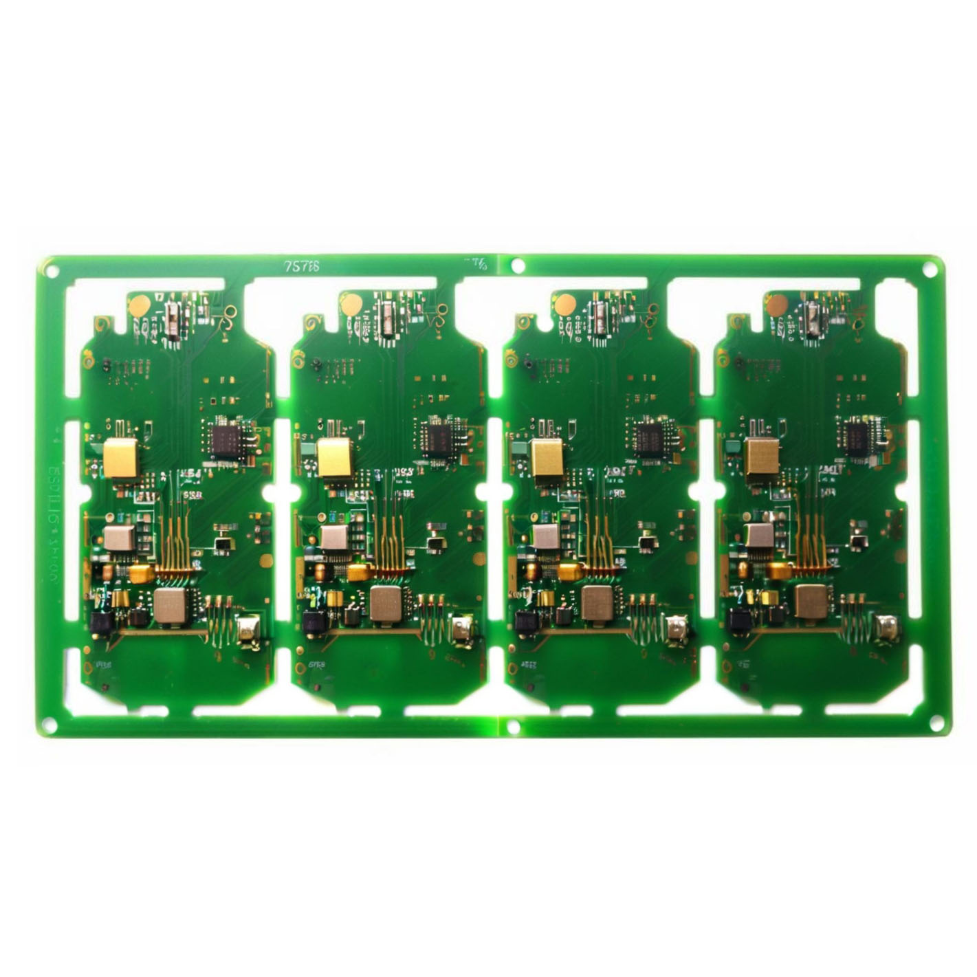
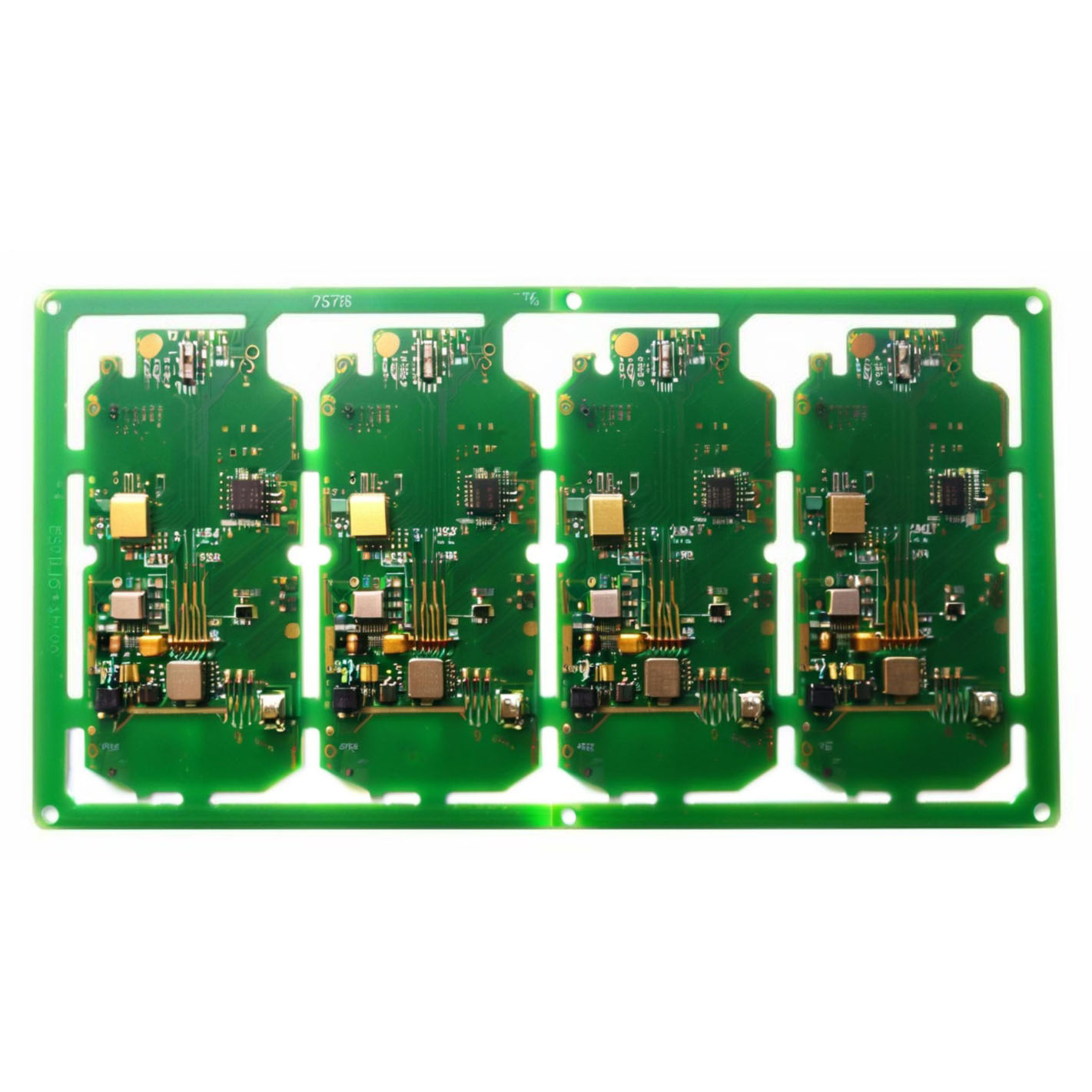
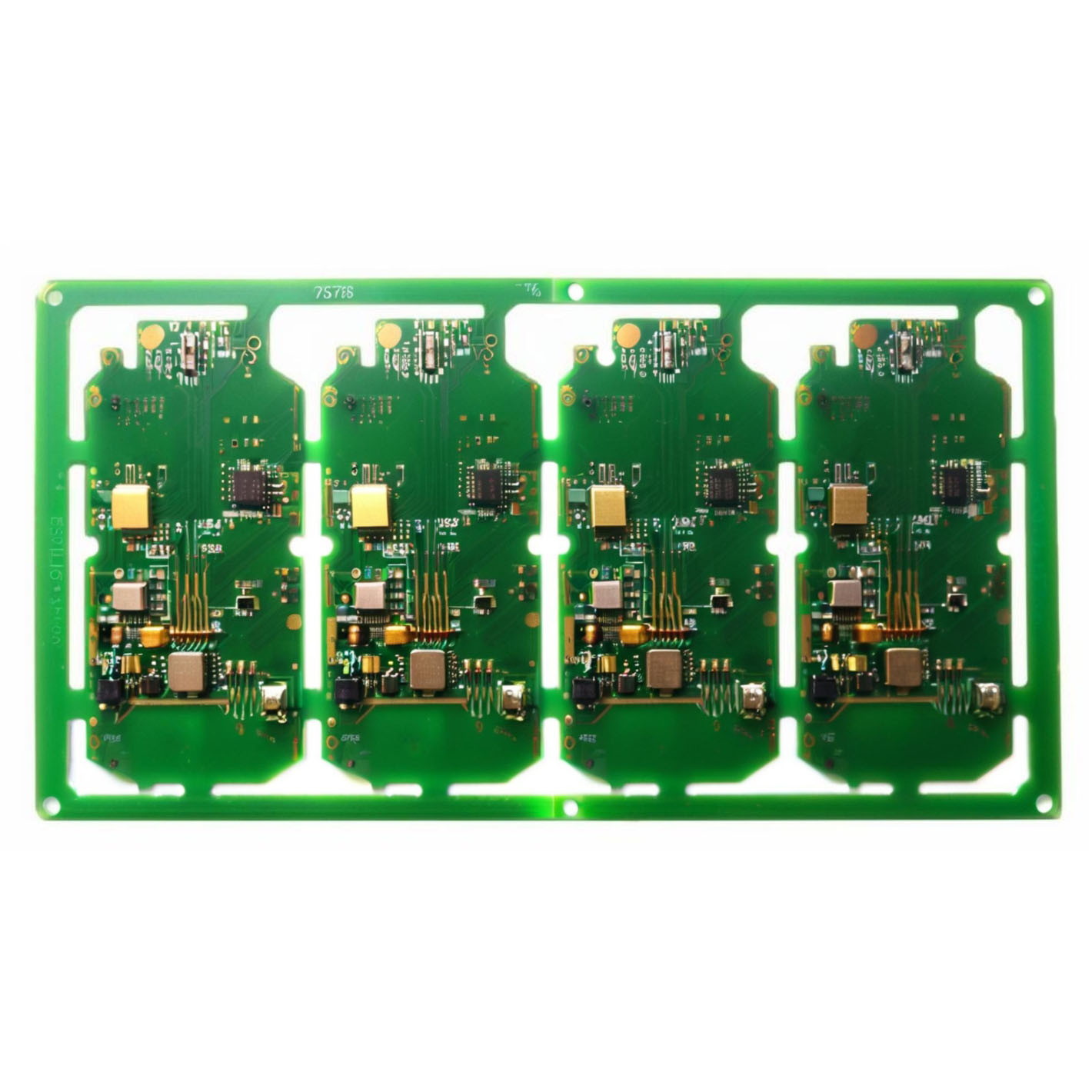
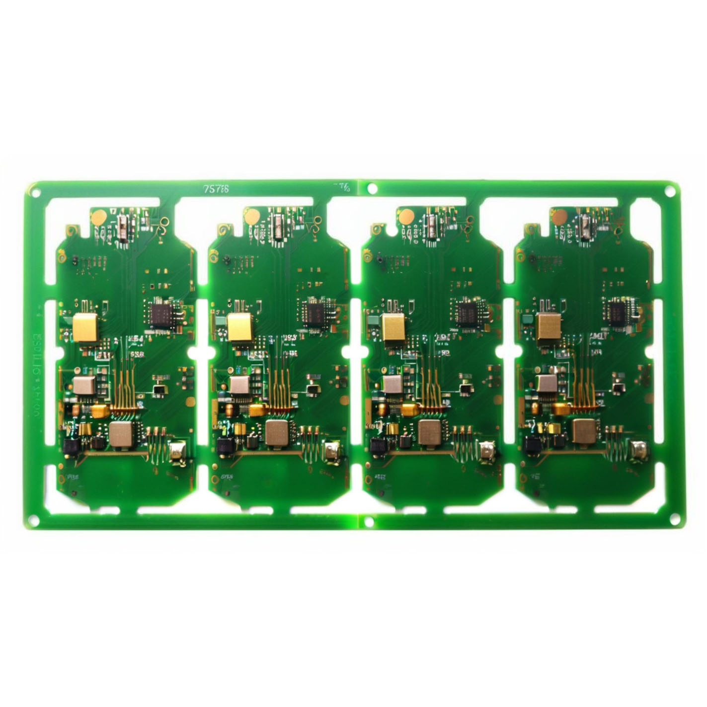


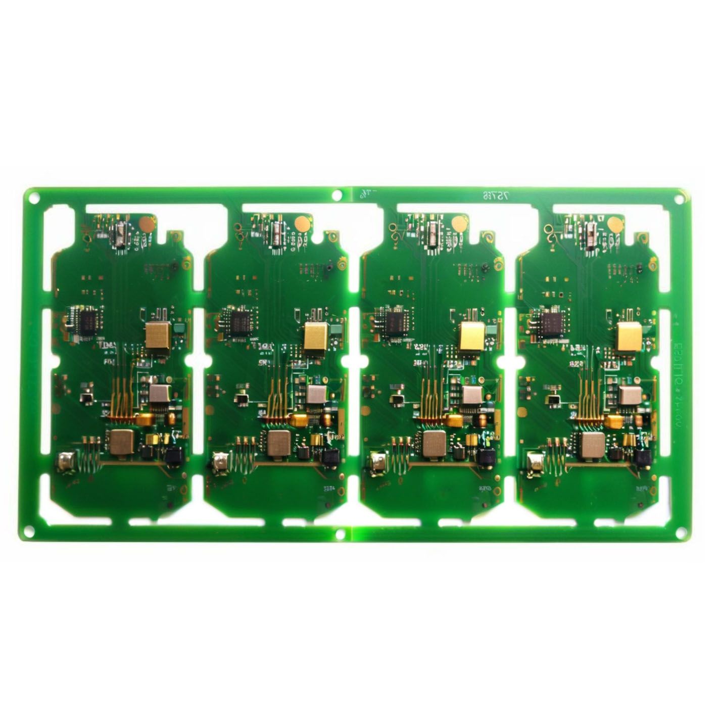
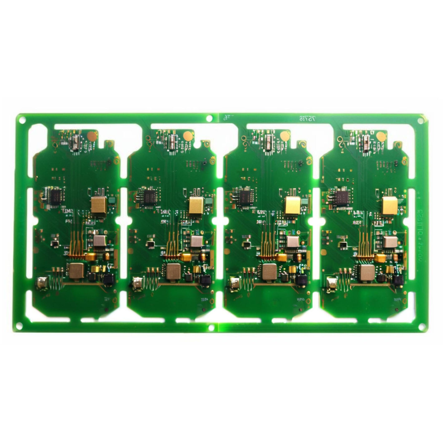
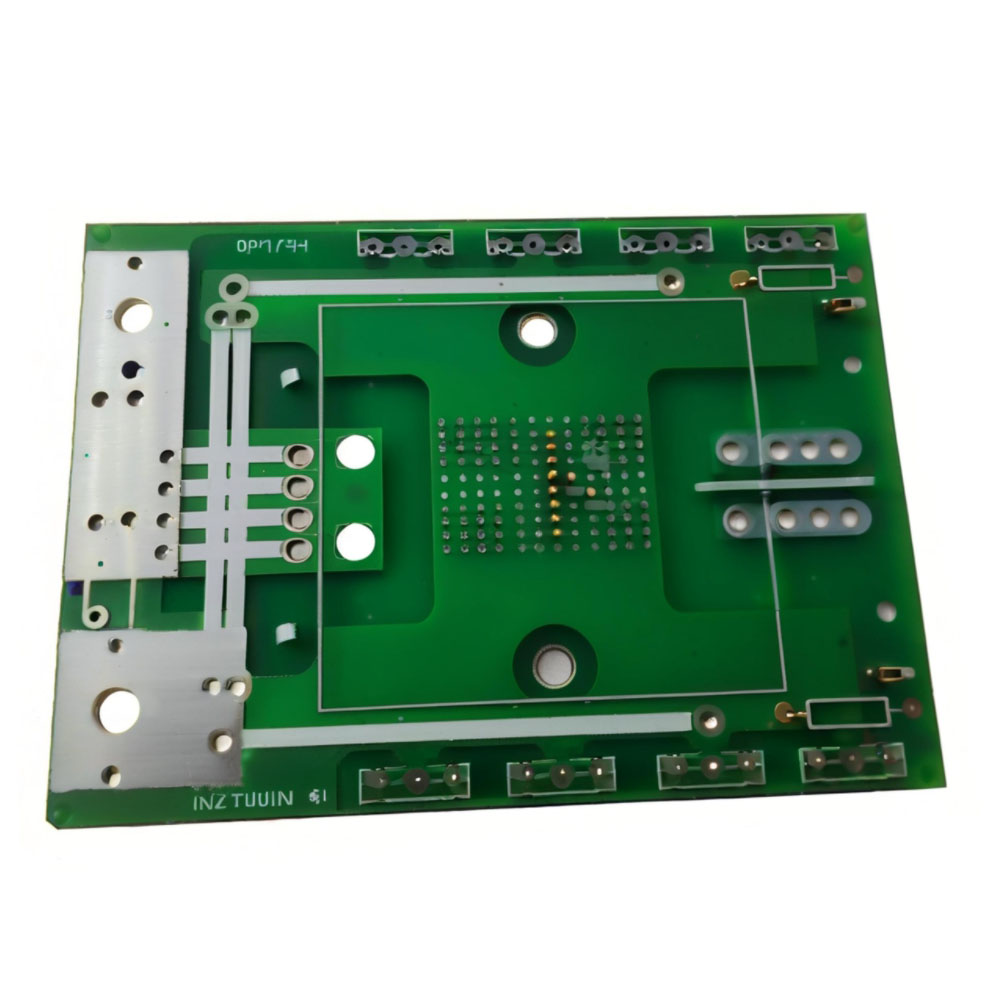
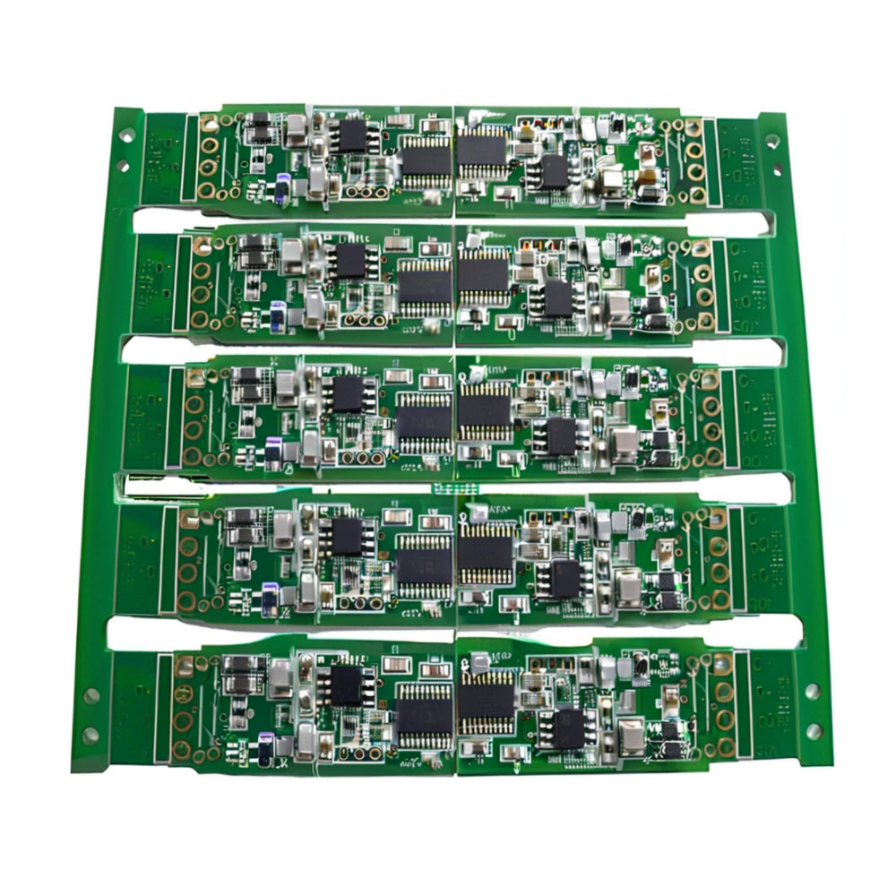
PCB Gerber File Design, PCBA Bom Gerber Files Design,Gerber PCB One Stop सेवाएं
उत्पाद विवरण:
- वोल्टेज एंड्योरेंस up to 3kV (as per material spec)
- टेस्ट
- न्यूनतम। लाइन की चौड़ाई 0.075mm (3mil)
- बोर्ड का प्रकार
- सिल्कस्क्रीन
- ज्वाला प्रतिरोध स्तर UL94-V0
- छेद का आकार Min. 0.15mm, Drilled as per spec
- Click to view more
X
मूल्य और मात्रा
- 1
- आईएनआर
उत्पाद की विशेषताएं
- Controlled Impedance available
- up to 600mm x 1200mm
- UL94-V0
- 0.4mm-3.2mm
- PCB Gerber File Design, PCBA BOM Gerber Files Design, Gerber PCB One Stop सेवाएं
- >= 10^12
- up to 3kV (as per material spec)
- 1-3 oz (as per design requirement)
- As per BOM (Bill of Materials)
- 0.075mm (3mil)
- Available on request
- 0.075mm (3mil)
- Min. 0.15mm, Drilled as per spec
- Gerber, BOM, Pick and Place, Centroid Files
- Vacuum Packing, Bubble Wrap, Custom Packaging
- Altium, Eagle, KiCad, OrCAD, Mentor, Gerber RS-274X
- Full batch and lot traceability
- Available (RoHS Compliant)
- Available on request
- Prototype to Mass Production
- 610mm x 1200mm
- 24 hours for prototypes, 5-7 days for mass production
- FOB, CIF, DDP, Door to Door
- Full Customization Supported
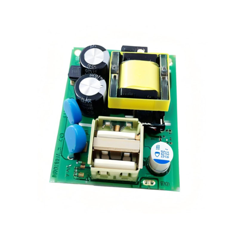
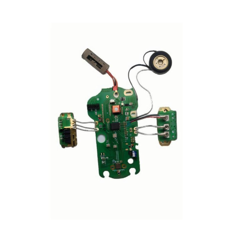
- SMT, Through-hole, Mixed Assembly, Complete Product Assembly
- 0.1mm
- Consigned, Turnkey, or Partial Turnkey
Tell us about your requirement

Price: Â
Quantity
Select Unit
- 50
- 100
- 200
- 250
- 500
- 1000+
Additional detail
मोबाइल number
Email

पीसीबीए अनुकूलित अन्य उत्पाद
सम्पर्क करने का विवरण
- नंबर 1506,15 मंजिल, एसएसजी टॉवर, 561 एडीएन बिएन फु स्ट्रीट, वार्ड 25, बिन्ह थान जिला, एचसीएमसी,हो ची मिन्ह सिटी - 717000, थान्ह फो हो ची मिन्ह, वियतनाम
- सुश्री टिफ़नी (थाओ गुयेन) (बिक्री खाता प्रबंधक)
- मोबाइल : +8613751081371
- जांच भेजें
नोवा टेक्नोलॉजी वियतनामी कंपनी लिमिटेड
|


NOVA TECHNOLOGY VIETNAMESE COMPANY LIMITED
सर्वाधिकार सुरक्षित.(उपयोग की शर्तें)
इन्फोकॉम नेटवर्क प्राइवेट लिमिटेड . द्वारा विकसित एवं प्रबंधित
इन्फोकॉम नेटवर्क प्राइवेट लिमिटेड . द्वारा विकसित एवं प्रबंधित
