


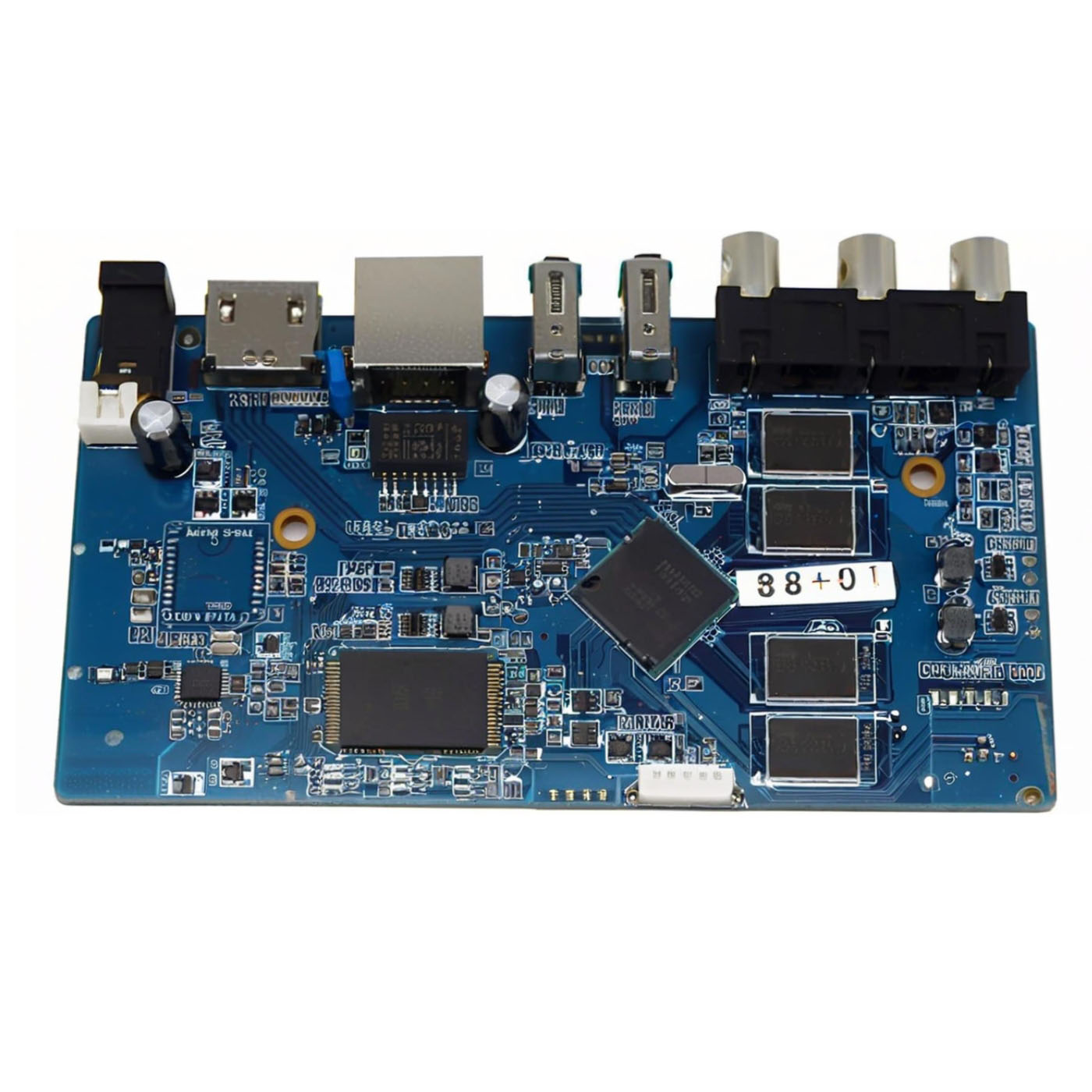


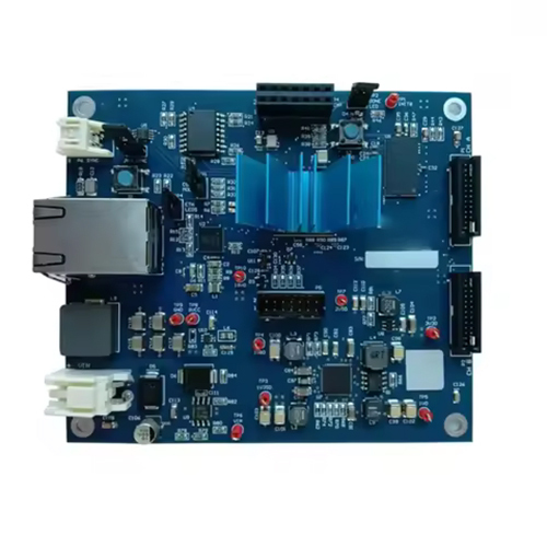
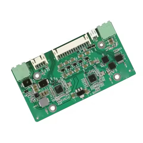
One-stop service manufacturers ENIG and OSP 3 stage HDI pcb for 5G Internet of Things Custom Supplier
उत्पाद विवरण:
- वोल्टेज एंड्योरेंस >1.5kV
- न्यूनतम। लाइन स्पेसिंग 0.075mm (3mil)
- बोर्ड का प्रकार
- छेद का आकार Min 0.1mm (laser), 0.2mm (mechanical)
- सोल्डर मास्क
- टेस्ट
- न्यूनतम। लाइन की चौड़ाई 0.075mm (3mil)
- Click to view more
X
मूल्य और मात्रा
- आईएनआर
- 1
उत्पाद की विशेषताएं
- 0.8mm - 2.0mm (custom available)
- >10^8
- >1.5kV
- 457mm x 610mm max
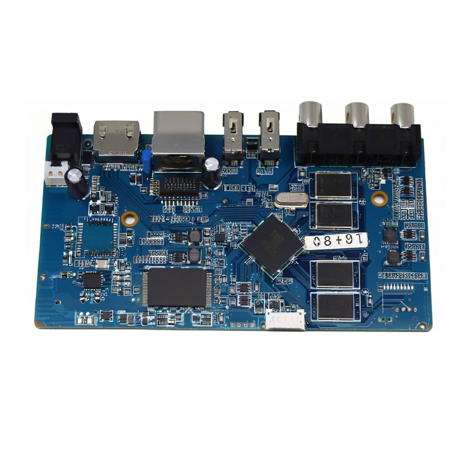
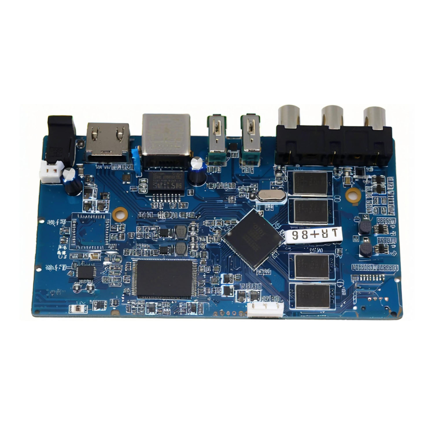
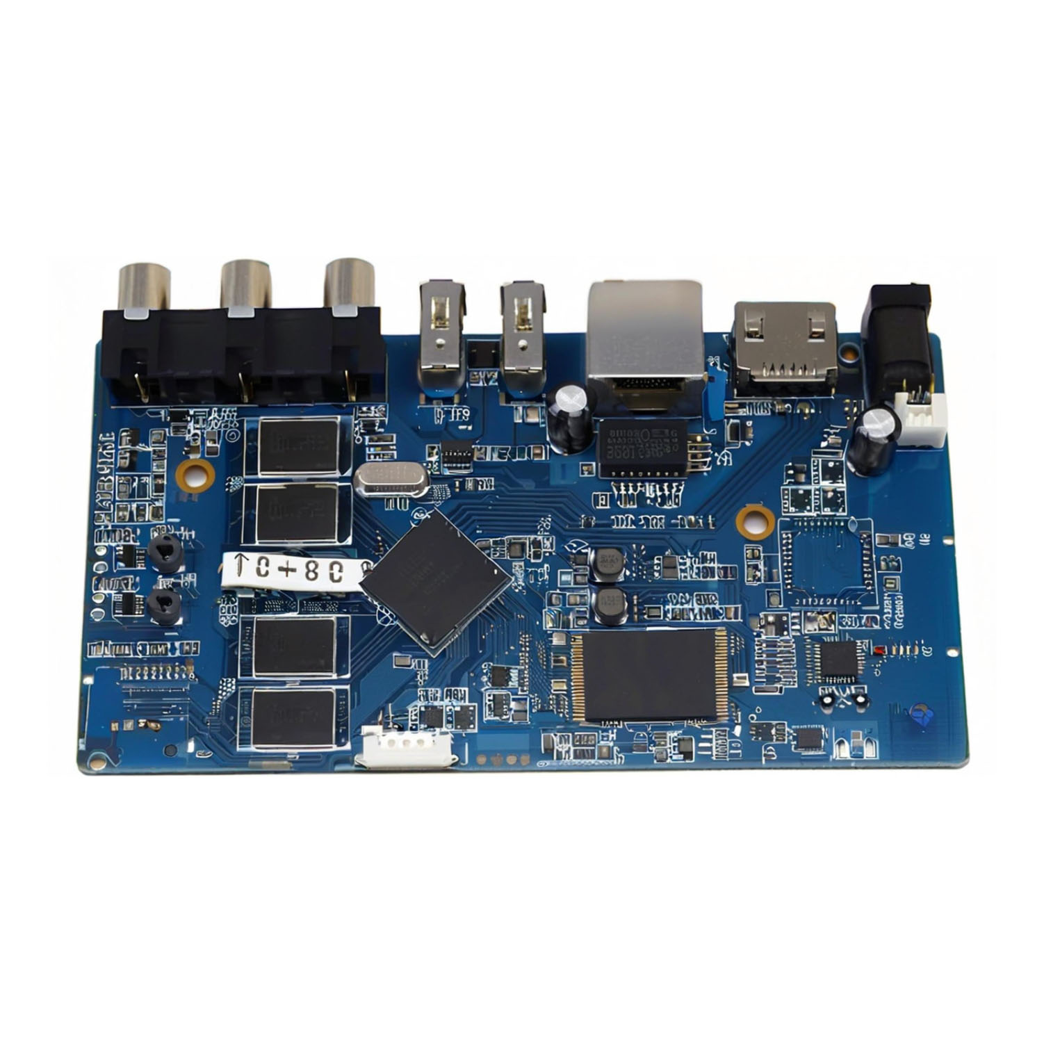
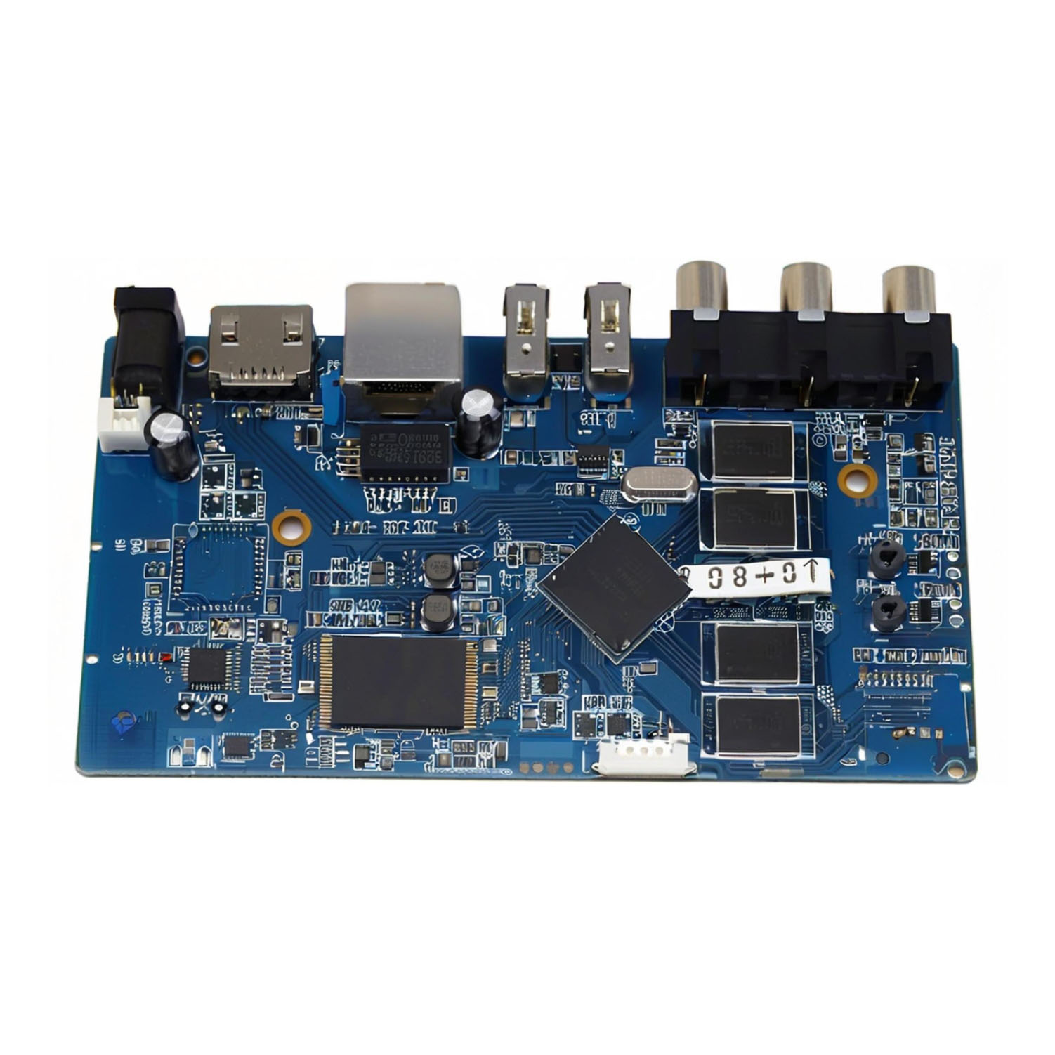
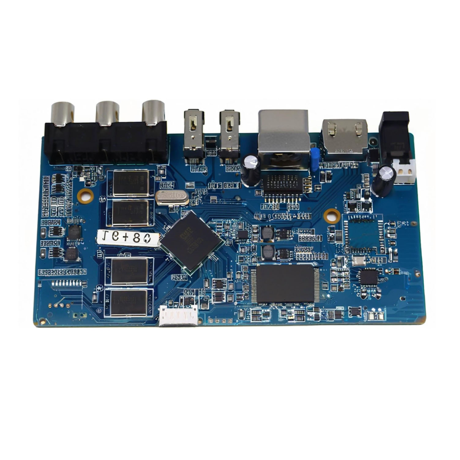
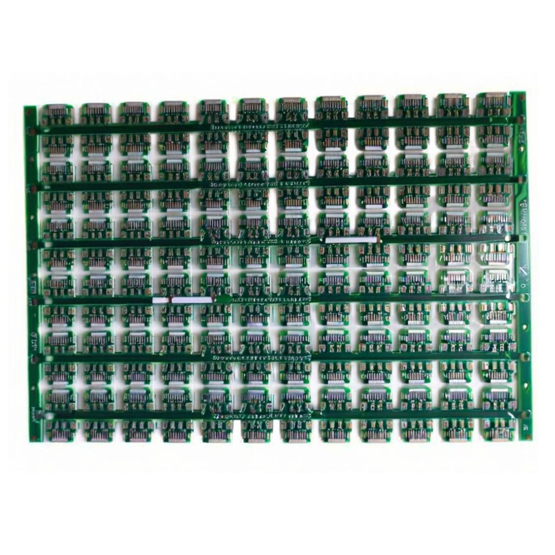
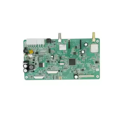
- 3 Stage HDI PCB
- 0.075mm (3mil)
- 1oz (35m), customizable
- Min 0.1mm (laser), 0.2mm (mechanical)
- 10% Controlled
- Not included (bare PCB), assembly available
- UL94 V-0
- Optional, customized support
- 0.075mm (3mil)
- Quick turn: 5-7 days
- Optimized for high-speed
- Yes
- Supported (layout, material, stackup)
- One-stop OEM/ODM, prototyping, mass production
- Laser microvia, stacked via, via-in-pad capability
- BGA, QFN, Fine-pitch supported
- 0.1mm
- -40C to +130C
- 5G Internet of Things, wireless communication, networking equipment
- 0.4m after ENIG
- ISO9001, UL, RoHS
- Custom laser / mechanical buildup
- IPC Class 2 / Class 3 available
- Vacuum sealed, ESD & moisture sensitive packaging
Tell us about your requirement

Price: Â
Quantity
Select Unit
- 50
- 100
- 200
- 250
- 500
- 1000+
Additional detail
मोबाइल number
Email

5जी आईओटी पीसीबीए अन्य उत्पाद
सम्पर्क करने का विवरण
- नंबर 1506,15 मंजिल, एसएसजी टॉवर, 561 एडीएन बिएन फु स्ट्रीट, वार्ड 25, बिन्ह थान जिला, एचसीएमसी,हो ची मिन्ह सिटी - 717000, थान्ह फो हो ची मिन्ह, वियतनाम
- सुश्री टिफ़नी (थाओ गुयेन) (बिक्री खाता प्रबंधक)
- मोबाइल : +8613751081371
- जांच भेजें
नोवा टेक्नोलॉजी वियतनामी कंपनी लिमिटेड
|


NOVA TECHNOLOGY VIETNAMESE COMPANY LIMITED
सर्वाधिकार सुरक्षित.(उपयोग की शर्तें)
इन्फोकॉम नेटवर्क प्राइवेट लिमिटेड . द्वारा विकसित एवं प्रबंधित
इन्फोकॉम नेटवर्क प्राइवेट लिमिटेड . द्वारा विकसित एवं प्रबंधित
