


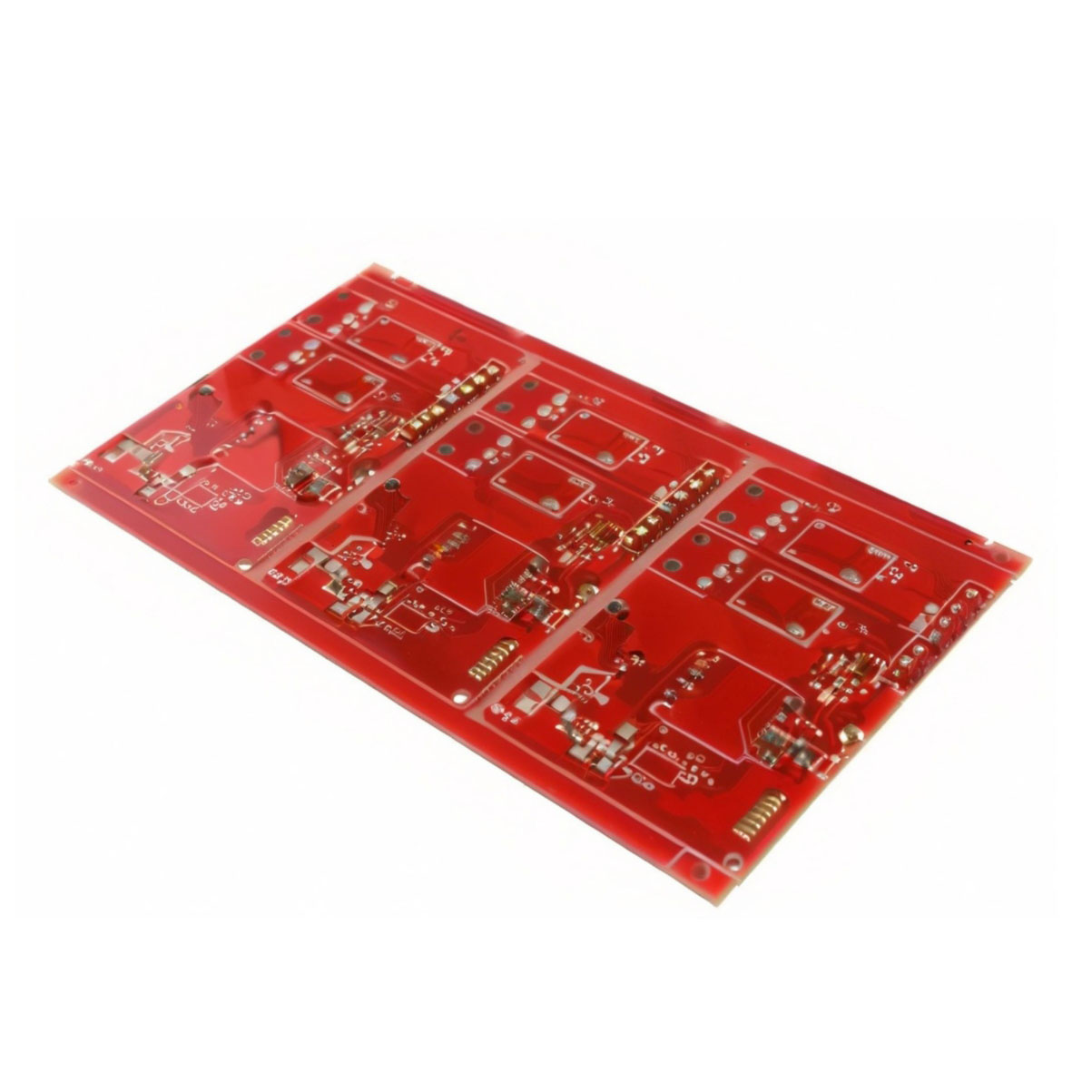


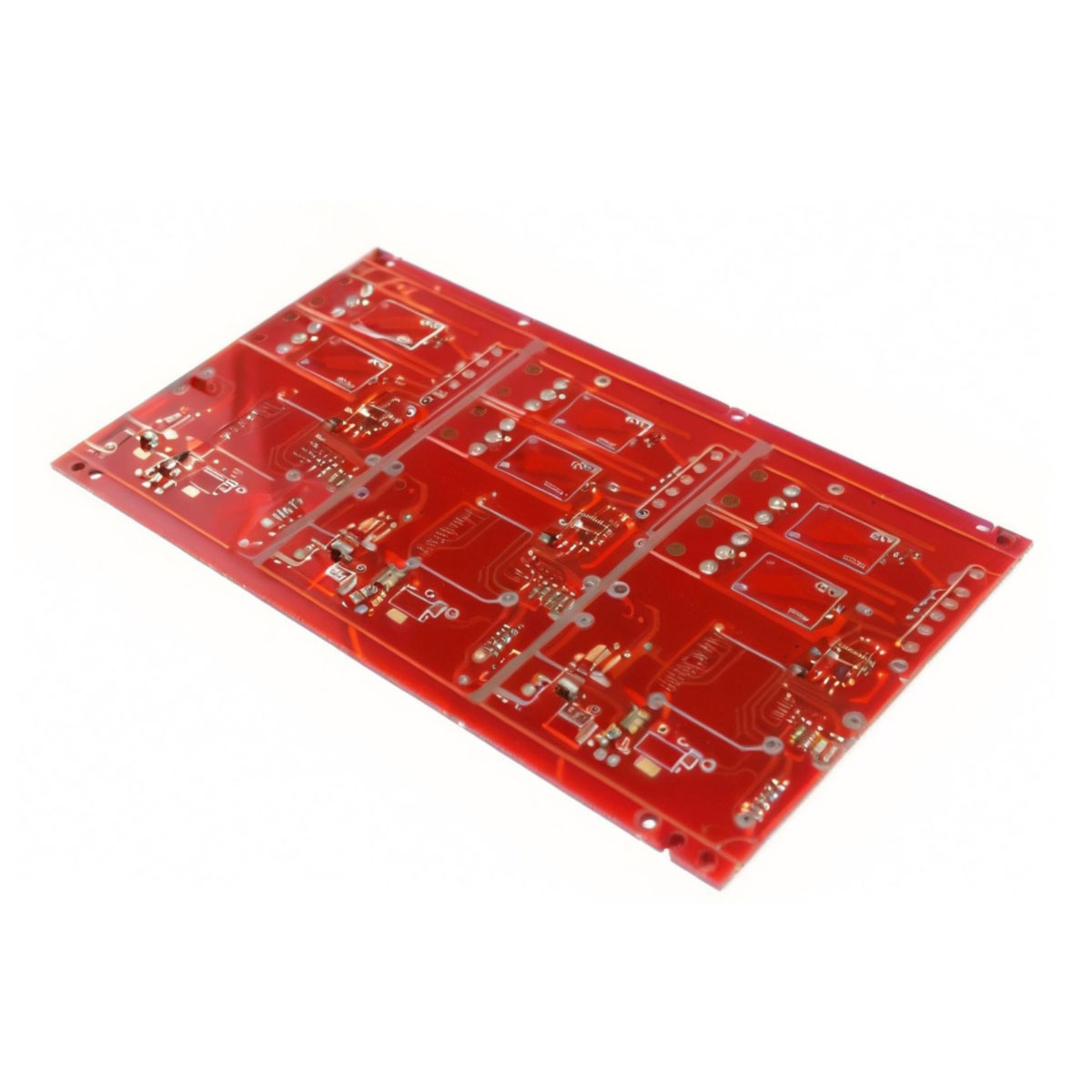
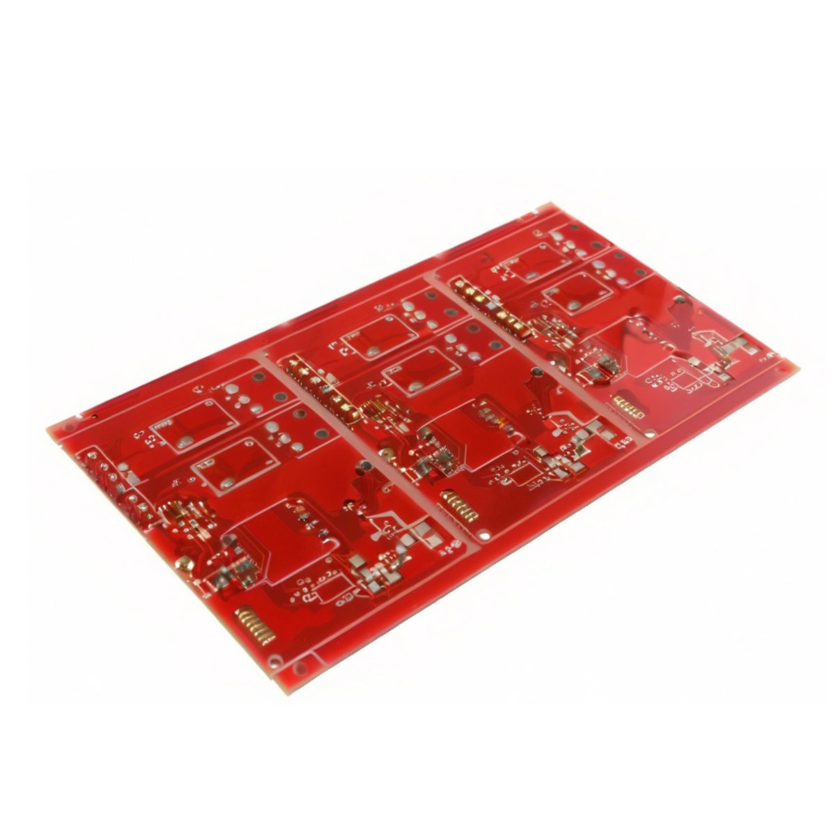

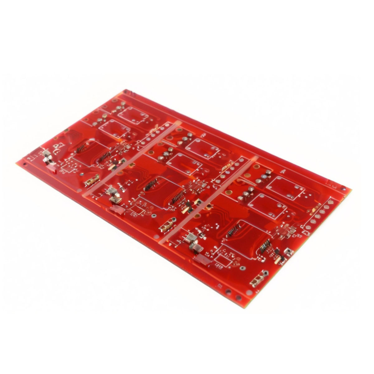
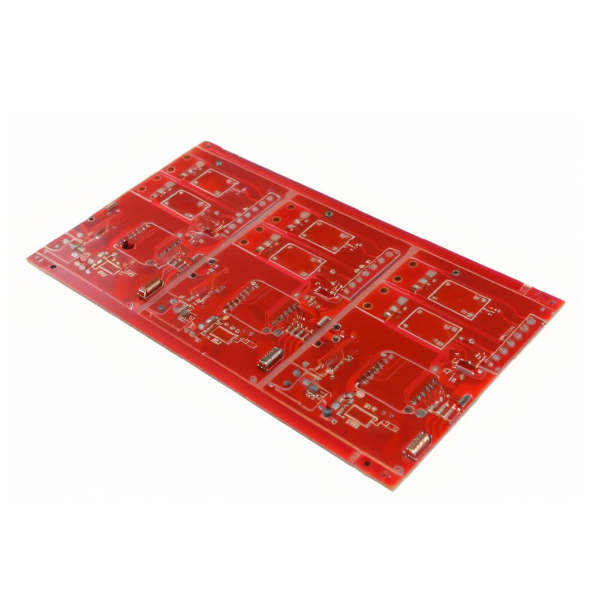


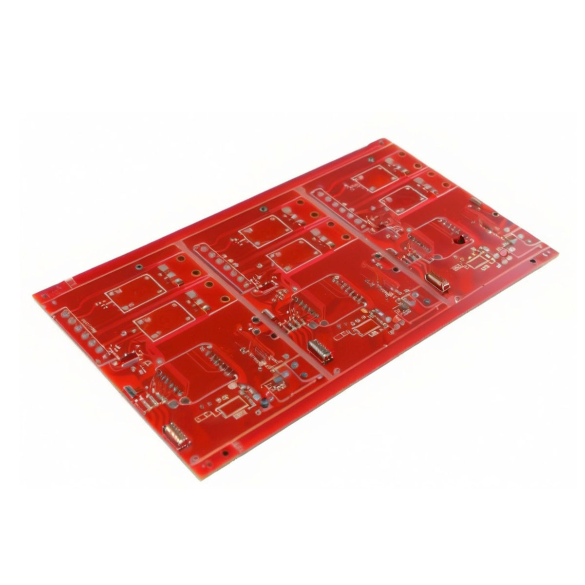
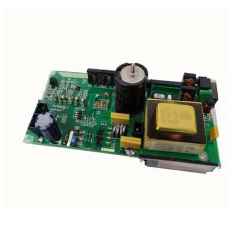
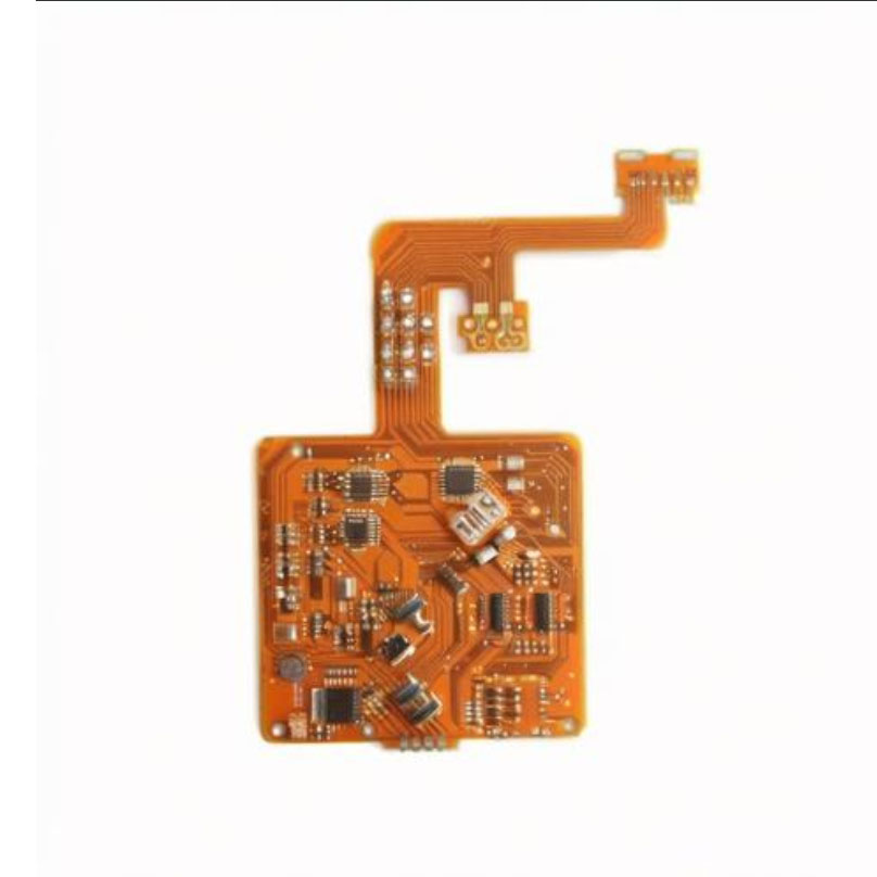
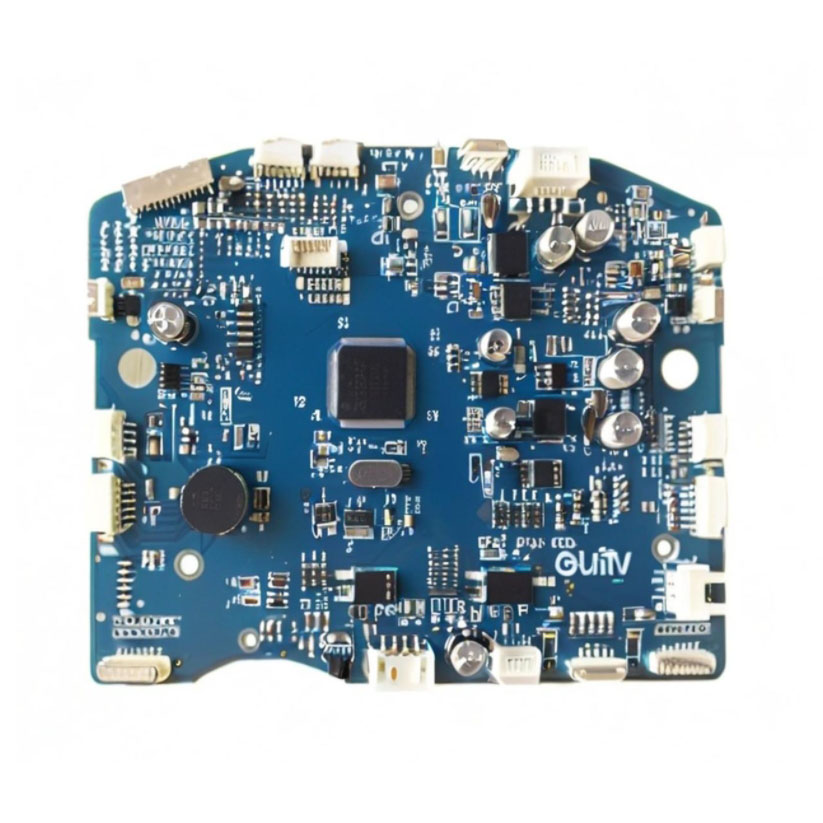
Multilayer Printed circuit board PCBA manufacture assembly Custom pcb design PCBA lay out design suppliers
उत्पाद विवरण:
- टेस्ट
- छेद का आकार Minimum 0.2mm
- सोल्डर मास्क
- न्यूनतम। लाइन स्पेसिंग 0.075mm
- प्रतिबाधा +/-10%
- बोर्ड का प्रकार
- इन्सुलेशन प्रतिरोध >10^12
- Click to view more
X
मूल्य और मात्रा
- 1
- आईएनआर
उत्पाद की विशेषताएं
- Custom/Up to 600mm x 1200mm
- >10^12
- SMT & Through-hole Assemblies
- Multilayer Printed Circuit Board (PCBA)
- Minimum 0.2mm
- UL94-V0
- 0.4mm~3.2mm
- 1500V AC/min
- 0.075mm
- 0.075mm
- 1oz (35m)~3oz (105m)
- +/-10%
- Optional integration
- Lead-Free and Lead options available
- ESD, Vacuum, Customized on request
- -40C to +130C
- Complete BOM management and sourcing
- Prototype & Mass Production
- Gold, Silver, Tin, OSP available
- as fast as 24-72 hours for prototypes
- Custom layout, Schematic & Gerber file support
- Industrial, Medical, Automotive, Consumer Electronics, Communication
- SMT, DIP, Mixed
Tell us about your requirement

Price: Â
Quantity
Select Unit
- 50
- 100
- 200
- 250
- 500
- 1000+
Additional detail
मोबाइल number
Email

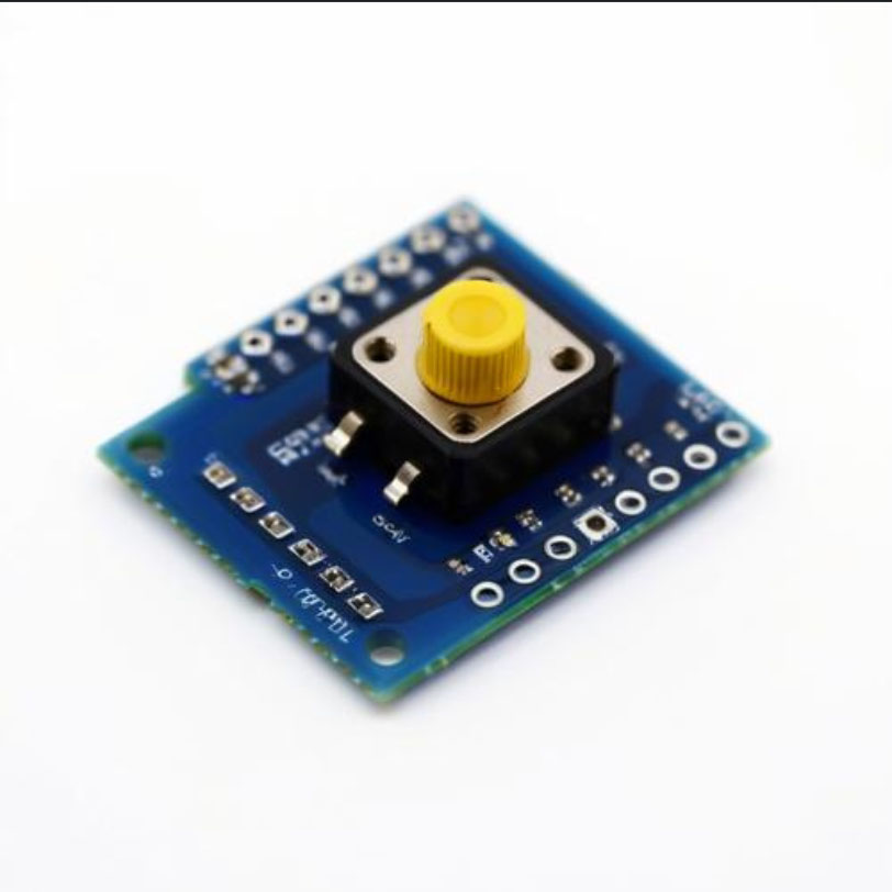
मल्टीलेयर पीसीबीए अन्य उत्पाद
सम्पर्क करने का विवरण
- नंबर 1506,15 मंजिल, एसएसजी टॉवर, 561 एडीएन बिएन फु स्ट्रीट, वार्ड 25, बिन्ह थान जिला, एचसीएमसी,हो ची मिन्ह सिटी - 717000, थान्ह फो हो ची मिन्ह, वियतनाम
- सुश्री टिफ़नी (थाओ गुयेन) (बिक्री खाता प्रबंधक)
- मोबाइल : +8613751081371
- जांच भेजें
नोवा टेक्नोलॉजी वियतनामी कंपनी लिमिटेड
|


NOVA TECHNOLOGY VIETNAMESE COMPANY LIMITED
सर्वाधिकार सुरक्षित.(उपयोग की शर्तें)
इन्फोकॉम नेटवर्क प्राइवेट लिमिटेड . द्वारा विकसित एवं प्रबंधित
इन्फोकॉम नेटवर्क प्राइवेट लिमिटेड . द्वारा विकसित एवं प्रबंधित
