


2 layer pcb printed circuit board and multilayer layer pcb pcba Design and assembly manufactur
उत्पाद विवरण:
- सिल्कस्क्रीन
- न्यूनतम। लाइन स्पेसिंग 0.1 mm
- न्यूनतम। लाइन की चौड़ाई 0.1 mm
- ज्वाला प्रतिरोध स्तर UL94-V0
- टेस्ट
- प्रतिबाधा Controlled Impedance available, 10%
- वोल्टेज एंड्योरेंस 250V to 3000V (depending on design)
- Click to view more
X
मूल्य और मात्रा
- आईएनआर
- 1
- Gerber, ODB++, BOM, Pick & Place
- -40C to +130C
- up to 500 x 600 mm
- Anti-static, Dry Packing
- Turnkey, Consigned, or Partial Turnkey
- Header, Terminal, FPC, Others
- 1 piece (prototype to mass production)
- Pb-Free/RoHS Compliant and Leaded available
- SMT, DIP, Mixed Technology
- In-Circuit Test, Functional Test, X-ray (BGA)
- 2-7 days for prototypes, 7-15 days for mass production
उत्पाद की विशेषताएं
- 0.1 mm
- Customized as per design
- Min. 0.2 mm
- 0.1 mm
- 1 oz
- UL94-V0
- Controlled Impedance available, 10%
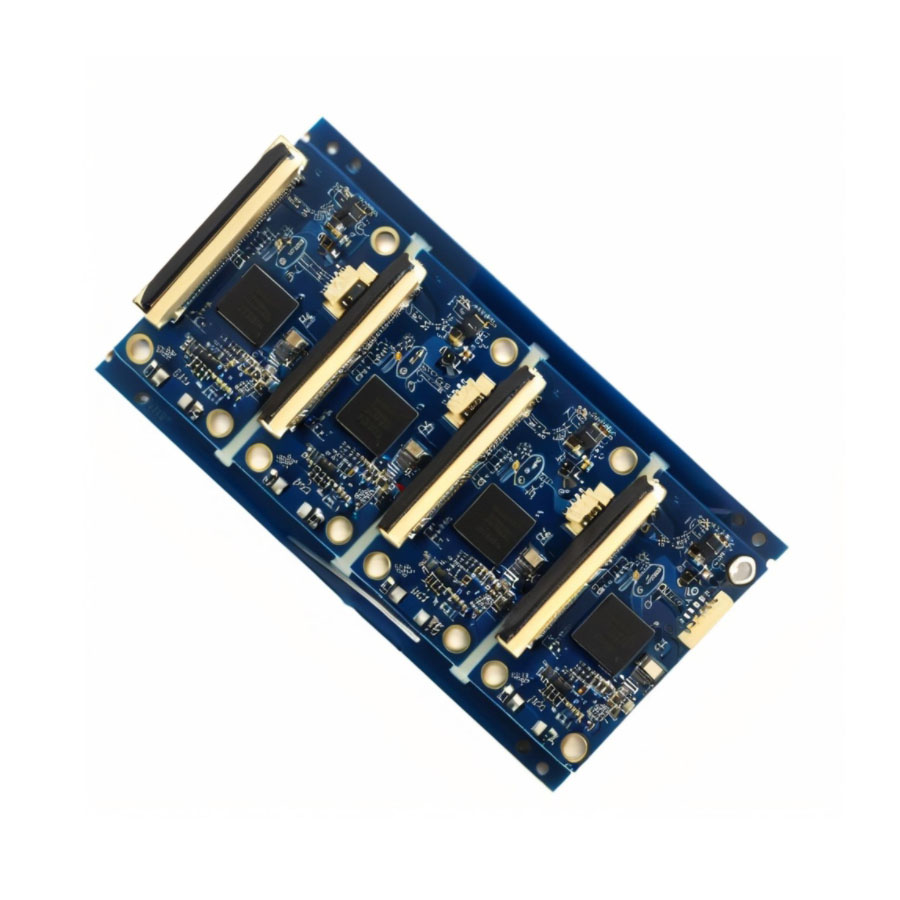
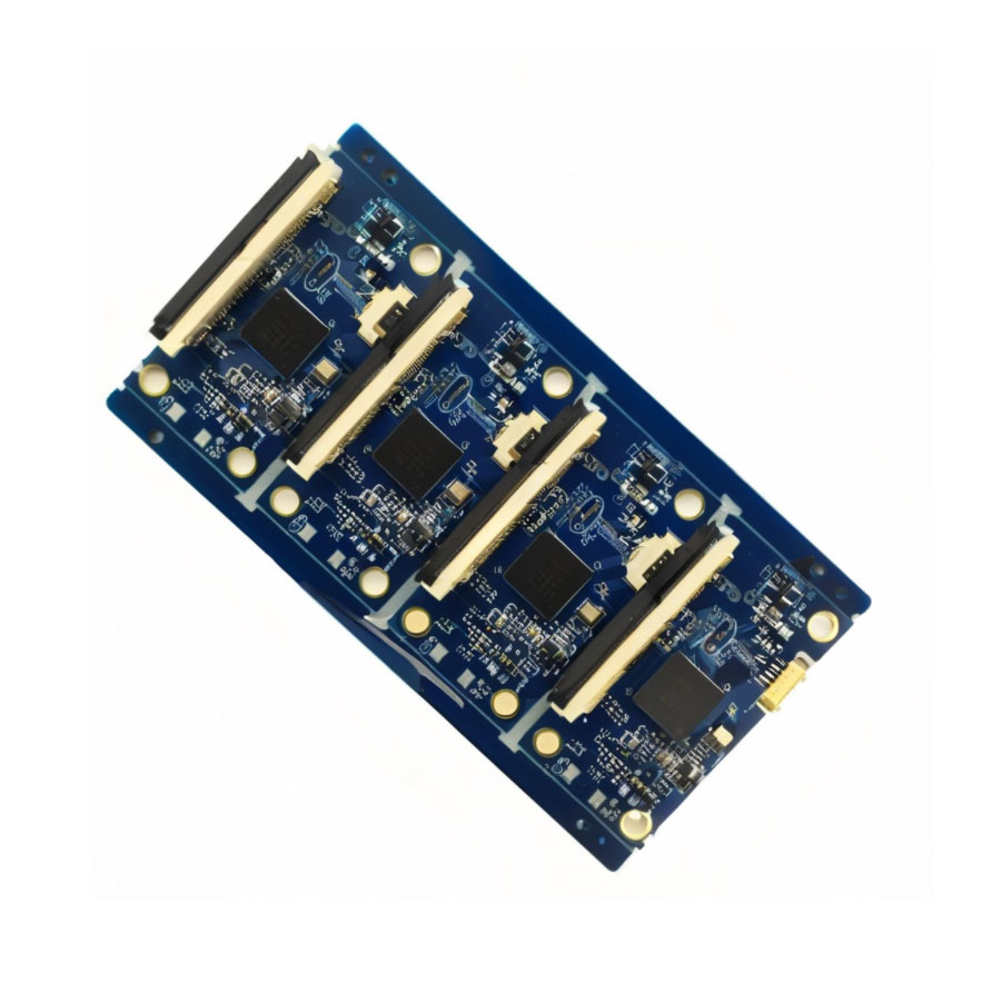
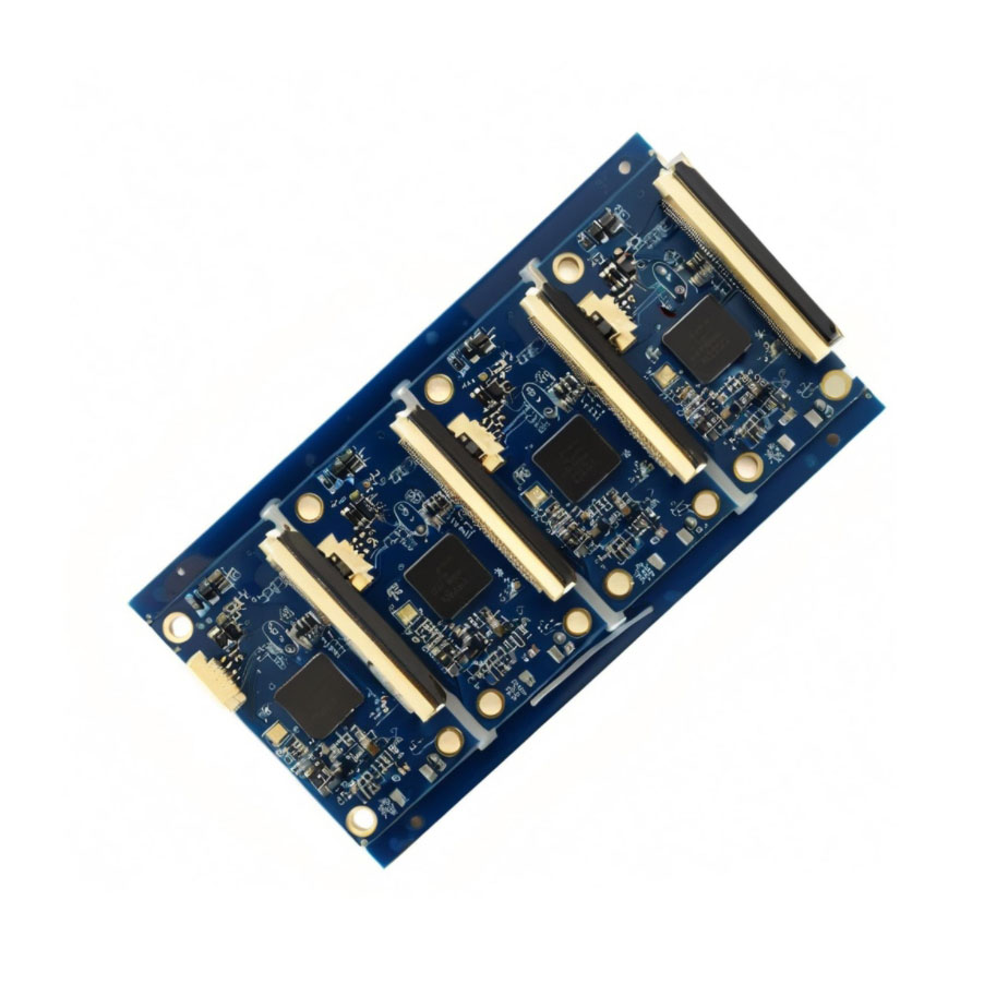
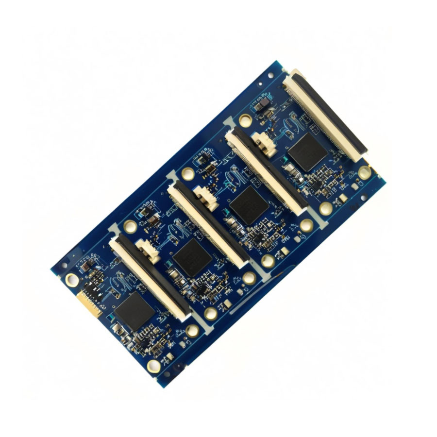
- 2 Layer PCB, Multilayer PCB, PCBA Design and Assembly
- 250V to 3000V (depending on design)
- SMT & Through-hole components as per BOM
- 1.6 mm
- >10^12
- Not included (customizable)
- Gerber, ODB++, BOM, Pick & Place
- -40C to +130C
- up to 500 x 600 mm
- Anti-static, Dry Packing
- Turnkey, Consigned, or Partial Turnkey
- Header, Terminal, FPC, Others
- 1 piece (prototype to mass production)
- Pb-Free/RoHS Compliant and Leaded available
- SMT, DIP, Mixed Technology
- In-Circuit Test, Functional Test, X-ray (BGA)
- 2-7 days for prototypes, 7-15 days for mass production
उत्पाद विवरण
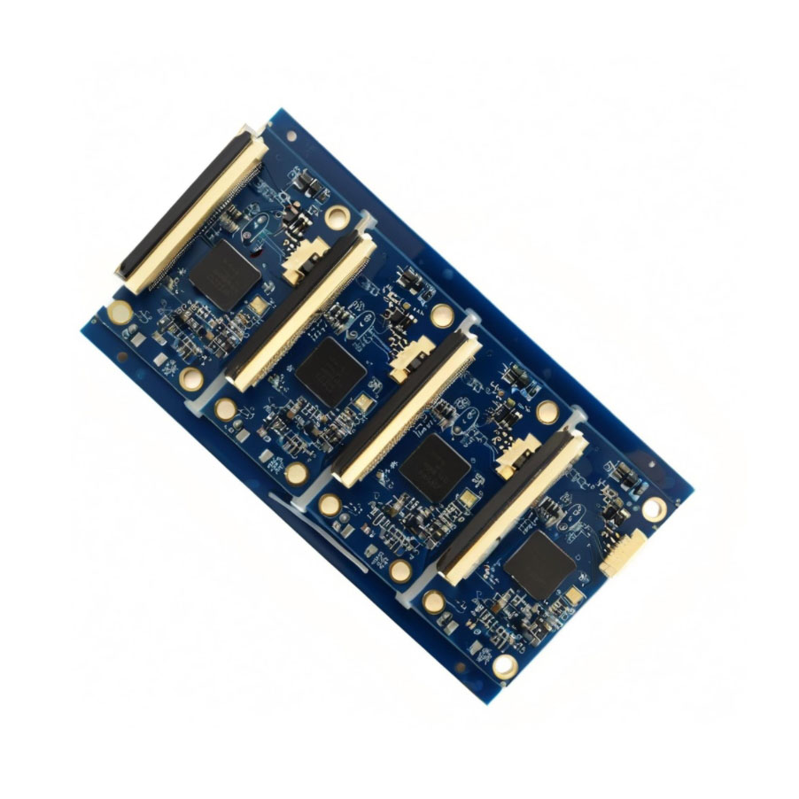
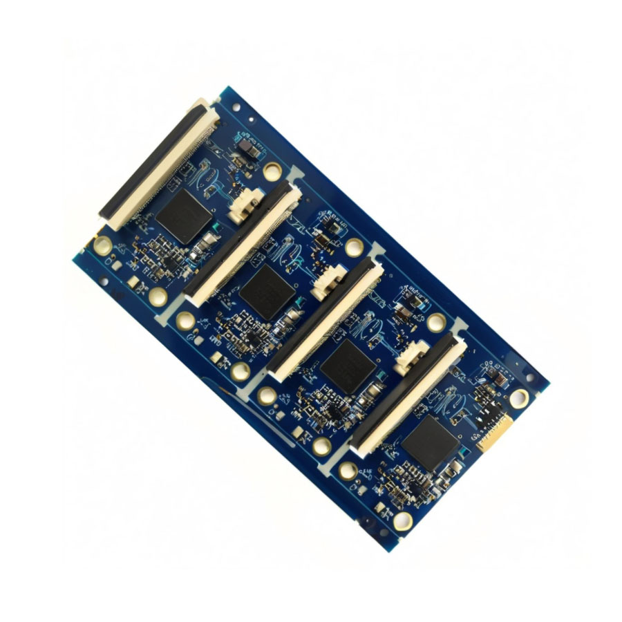
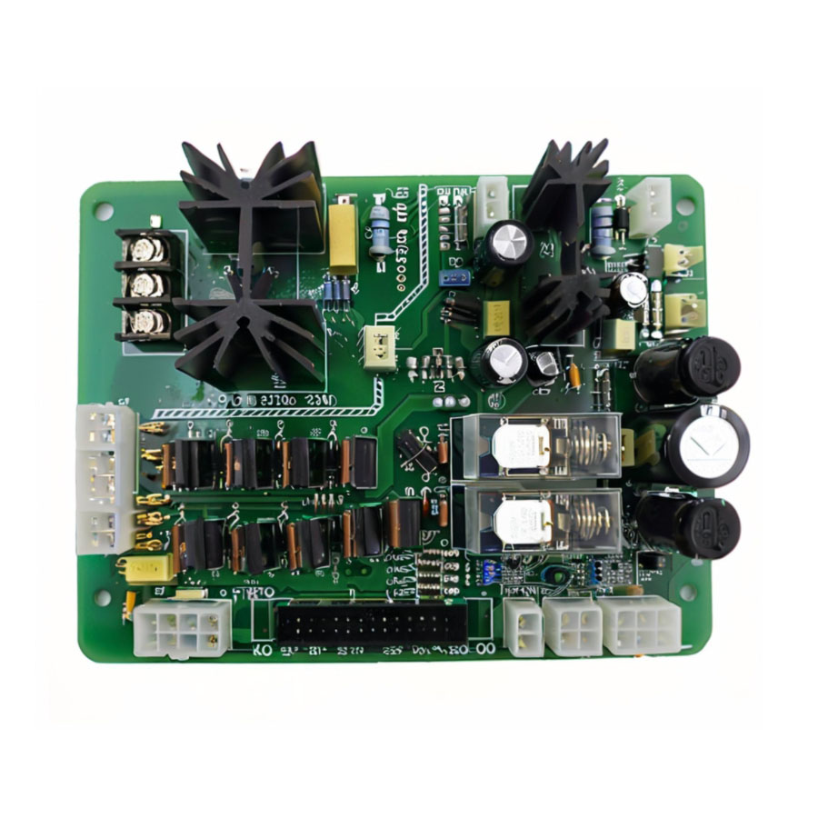
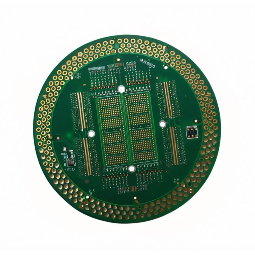
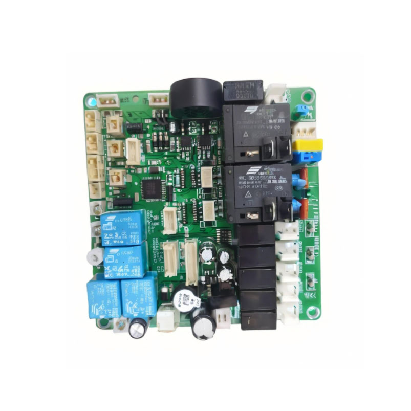
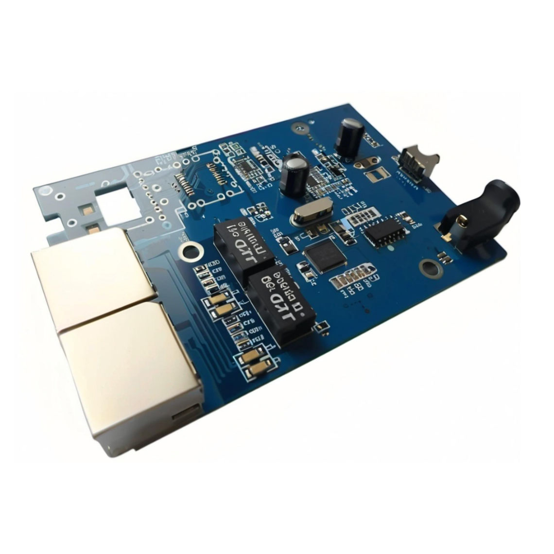
Discover an affordable yet formidable solution for your electronic projects with our sizzling 2-layer and multilayer PCB and PCBA design and assembly. Each board showcases magnificent engineering, manufactured under pristine quality control with a capacity of up to 16+ layers, minuscule 0.1 mm line spacing, and min. hole size of 0.2 mm. Benefit from scarce, state-of-the-art SMT, DIP, or Mixed Technology assembly while enjoying versatile component sourcing-Turnkey, Consigned, or Partial Turnkey. Supported by a wide range of surface finishes and high-performance base materials, every order receives 100% testing and strict anti-static, dry-packed delivery straight from India. Fast turnaround and full customization available.
Advanced Usage, Extra Features, and Applications
Our 2-layer and multilayer PCB and PCBA assemblies are ideal for both prototyping and mass production, tailored to suit industries from consumer electronics to automotive and industrial automation. Supporting advanced features like controlled impedance, AOI, X-ray (BGA) testing, and customizable soldermask coloring, your designs are safely realized with accuracy. Rigid and flexible PCB options cater to specialized sensor, communication, and power applications, ensuring versatile usage in demanding environments.
Supply Capabilities, Export Markets, and Sample Policy
With stock ready and scalable manufacturing, we ensure swift transportation and reliable freight services across principal export markets, notably in North America, Europe, and Asia. Our robust supply ability meets urgent demand from prototype to mass production. A flexible sample policy empowers clients to evaluate product quality before larger commitments, supporting seamless integration and expedited product launch cycles to meet ever-shifting industry requirements.
FAQ's of 2 layer pcb printed circuit board and multilayer layer pcb pcba Design and assembly manufactur:
Q: How quickly can I receive prototypes or mass production orders for PCBs?
A: Prototypes can be delivered within 2-7 days, while mass production orders typically ship in 7-15 days, ensuring rapid project progression regardless of order size.Q: What industries commonly use your 2-layer and multilayer PCB and PCBA assemblies?
A: Our products are extensively applied in consumer electronics, automotive systems, industrial control, medical devices, and communication technology, offering reliable performance and customization for diverse sectors.Q: What is the process for turnkey or partial turnkey component sourcing?
A: With turnkey services, we procure all components, assemble, and test your PCBA, while partial turnkey allows you to supply select parts, enhancing flexibility and streamlining your supply chain.Q: Where do you export your PCBs, and do you support sample shipments internationally?
A: We supply our products globally, with strong export channels in North America, Europe, and Asia, and offer international sample shipments to facilitate product evaluation across regions.Q: What are the benefits of choosing your SMT, DIP, and Mixed Technology assembly types?
A: Our versatile assembly methods accommodate complex designs, allow for precise mounting of surface and through-hole components, and support intricate, multi-layered PCBs with enhanced durability and electrical performance.Q: How are the PCBs tested for quality before shipping?
A: Each board undergoes comprehensive testing, including 100% E-test, AOI, In-Circuit, Functional, and optional X-ray (for BGA), guaranteeing products meet stringent quality standards before shipment.Tell us about your requirement

Price: Â
Quantity
Select Unit
- 50
- 100
- 200
- 250
- 500
- 1000+
Additional detail
मोबाइल number
Email

मल्टीलेयर पीसीबीए अन्य उत्पाद
सम्पर्क करने का विवरण
- नंबर 1506,15 मंजिल, एसएसजी टॉवर, 561 एडीएन बिएन फु स्ट्रीट, वार्ड 25, बिन्ह थान जिला, एचसीएमसी,हो ची मिन्ह सिटी - 717000, थान्ह फो हो ची मिन्ह, वियतनाम
- सुश्री टिफ़नी (थाओ गुयेन) (बिक्री खाता प्रबंधक)
- मोबाइल : +8613751081371
- जांच भेजें
नोवा टेक्नोलॉजी वियतनामी कंपनी लिमिटेड
|
 मुझे निःशुल्क कॉल करें

NOVA TECHNOLOGY VIETNAMESE COMPANY LIMITED
सर्वाधिकार सुरक्षित.(उपयोग की शर्तें)
इन्फोकॉम नेटवर्क प्राइवेट लिमिटेड . द्वारा विकसित एवं प्रबंधित
इन्फोकॉम नेटवर्क प्राइवेट लिमिटेड . द्वारा विकसित एवं प्रबंधित
