


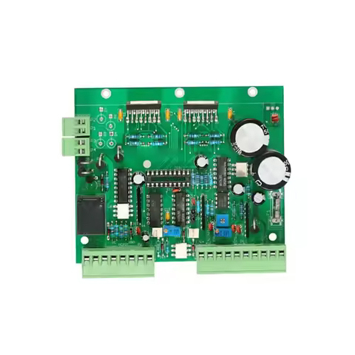
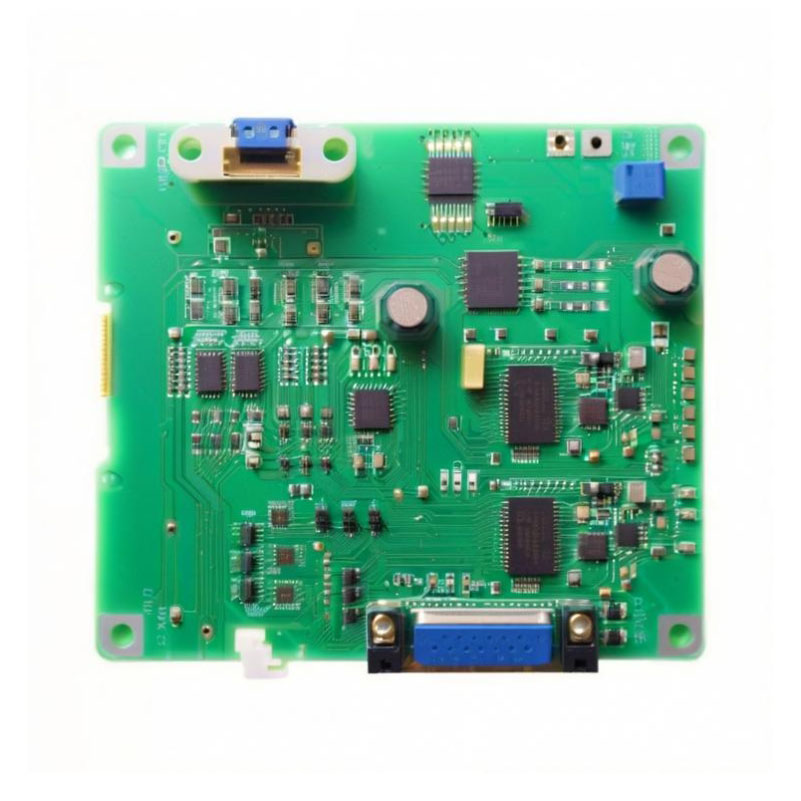
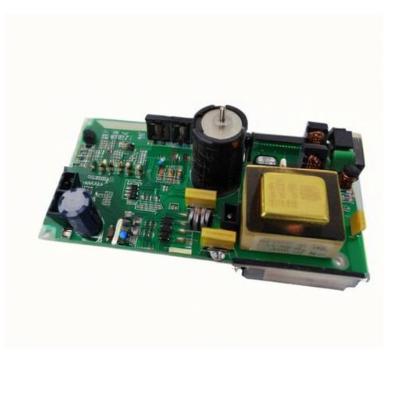
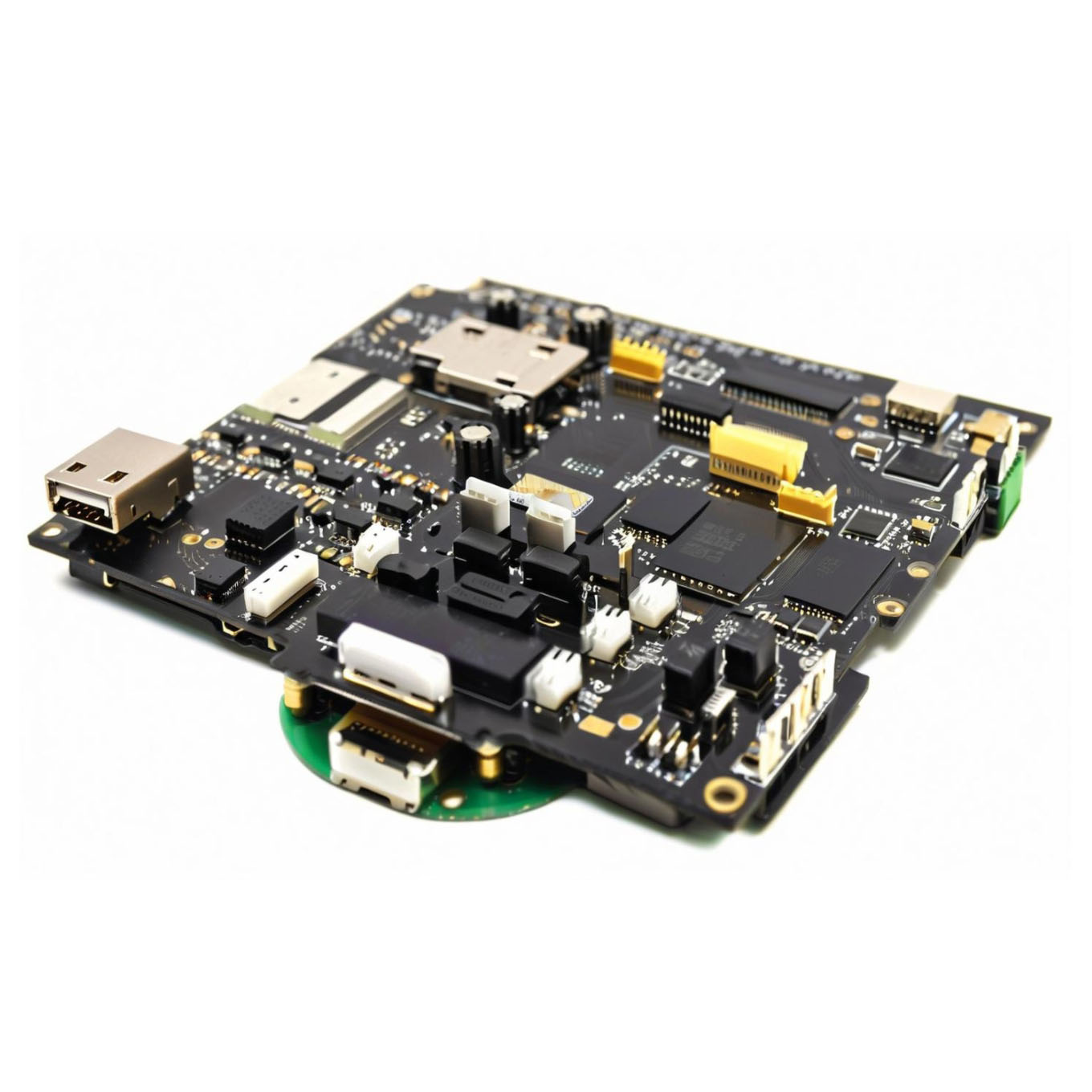
Customize PCB Manufacturer Multilayer Manufacturing 4 Layers ENIG PCB Layout Design Services Prototype Multilayer PCB
Product Details:
- Hole Size Minimum 0.2mm
- Test 100% E-test, AOI
- Voltage Endurance 1.3KV
- Flame Resistance Level UL94-V0
- Impedance Controlled impedance available
- Silkscreen White (both sides optional)
- Board Type Prototype PCB, Multilayer PCB
- Click to view more
X
Customize PCB Manufacturer Multilayer Manufacturing 4 Layers ENIG PCB Layout Design Services Prototype Multilayer PCB Price And Quantity
- 1
- INR
- SMT & Through Hole
- Halogen Free available
- Up to 600mm x 1200mm
- Gold/Au plating on pads optional
- Vacuum Pack + Carton
- 1 Piece (Prototype Support)
- Gerber, ODB++, Eagle, Altium Supported
- Yes
- Yes
- Electronic Devices, Industrial Controls, Communication Equipment
- Available upon request
- Prototype in 3-7 days
- Custom PCB Layout Design Service Supported
Customize PCB Manufacturer Multilayer Manufacturing 4 Layers ENIG PCB Layout Design Services Prototype Multilayer PCB Product Specifications
- UL94-V0
- White (both sides optional)
- 1.6mm (customizable range 0.4mm-3.2mm)
- Controlled impedance available
- 1.3KV
- 100% E-test, AOI
- Green (custom color available)
- Minimum 0.2mm
- Multilayer PCB
- >10^12
- Not included
- ENIG (Electroless Nickel Immersion Gold)
- 0.1mm
- FR4, High TG FR4 optional
- 0.1mm
- Custom size as per design
- 4 Layers
- 1oz (can be customized)
- Prototype PCB, Multilayer PCB
- SMT & Through Hole
- Halogen Free available
- Up to 600mm x 1200mm
- Gold/Au plating on pads optional
- Vacuum Pack + Carton
- 1 Piece (Prototype Support)
- Gerber, ODB++, Eagle, Altium Supported
- Yes
- Yes
- Electronic Devices, Industrial Controls, Communication Equipment
- Available upon request
- Prototype in 3-7 days
- Custom PCB Layout Design Service Supported
Product Description
Explore next-level innovation with our Customize PCB Manufacturer services, offering Polished and Dazzling 4-layer ENIG PCBs. Crafted for crackerjack performance, our prototypes are perfect for electronic devices, industrial controls, and communication equipment. Pick yours and grab the advantage of customized layouts, thermal shock resistance, and gold finishing. With options for RoHS compliance, controlled impedance, and various sizes, our boards are flawlessly designed to suit your specific needs. Fast lead times, thorough E-testing, and customizable options await-grab yours today and elevate your projects!
Applications and Key Uses for Our Multilayer ENIG PCBs
Our 4-layer ENIG PCB layout design services are engineered for a variety of applications-electronic devices, industrial control panels, and communication equipment being prime examples. Use type includes prototype to production quantities, providing flexibility for innovators and manufacturers. The application surface is vacuum-packed with quality assurance and supports SMT & through-hole mounting, catering to high-performance needs. With robust specifications and polished finishing, these PCBs fit the demands of dynamic electronics environments.
Order Processing, Domestic Market Focus, and Packing Details
Order completion is streamlined with a focus on the main domestic market across India. Our order processing ensures rapid turnaround, with prototypes ready in 3-7 days. Packaging highlights include vacuum packing along with secure carton boxing, guaranteeing product safety up to delivery. Our FOB port is based in India, serving as a reliable hub for nationwide and export shipping; domestic mar is prioritized for quick distribution, making order fulfillment and customer satisfaction our top priorities.
FAQ's of Customize PCB Manufacturer Multilayer Manufacturing 4 Layers ENIG PCB Layout Design Services Prototype Multilayer PCB:
Q: How do I start the process for custom 4-layer ENIG PCB manufacturing?
A: Begin by submitting your PCB design files in Gerber, ODB++, Eagle, or Altium formats. Our team will review, suggest optimizations if necessary, and prompt you for order confirmation to proceed with manufacturing.Q: What applications are best suited for these multilayer PCBs?
A: These PCBs are ideal for electronic devices, industrial controls, and communication equipment, particularly where high reliability, advanced interconnections, and robust thermal or electrical properties are required.Q: When can I expect my PCB prototype after confirming my order?
A: Once your order is confirmed, prototypes are typically shipped within 3-7 business days, ensuring quick turnaround for your project development needs.Q: Where can I get technical support on PCB design and specifications?
A: Our technical team offers ongoing support during design review and manufacturing. Assistance is available at all stages to address specification, layout, or material queries.Q: What are the benefits of using your ENIG-multilayer PCB services?
A: Our services provide customization, controlled impedance options, RoHS compliance, vacuum packaging, fast delivery, and comprehensive quality inspection, delivering reliable solutions for demanding electronic applications.Tell us about your requirement

Price:
Quantity
Select Unit
- 50
- 100
- 200
- 250
- 500
- 1000+
Additional detail
Mobile number
Email

Other Products in 'Multilayer PCBA' category
Contact Details
- No. 1506,15 Floor, SSG Tower, 561 ADien Bien Phu Str, Ward 25, Binh Thanh Dist, HCMC, Ho Chi Minh City - 717000, Thanh Pho Ho Chi Minh, Vietnam
- Ms. Yolanda Ke (Sales Account Manager)
- Mobile : +8613751081371
- Send Inquiry
NOVA TECHNOLOGY VIETNAMESE COMPANY LIMITED
|
 Call Me Free

NOVA TECHNOLOGY VIETNAMESE COMPANY LIMITED
All Rights Reserved.(Terms of Use)
Developed and Managed by Infocom Network Private Limited.
Developed and Managed by Infocom Network Private Limited.
